By Truechip Verification Team
ABSTRACT:
The article demonstrates the issue of multiple driver created on an interface signal due to clocking blocks while integrating the DUT and the testbench. A wrapper interface has been introduced which will serve as a medium for connecting the DUT and TB and it further prevents the creation of multiple driver on any interface signal.
INTRODUCTION:
The purpose of a testbench is to determine the correctness of the design under test (DUT) which is facilitated by generating the stimulus, applying stimulus to the DUT, capturing the response , checking for correctness and measuring progress against the overall verification goals. An Interface provides the mechanism of connecting the testbench to the DUT thereby encapsulating the communication between the DUT and the testbench.
The usage of Interfaces to connect the TB with the DUT has been predominant since we can add new connections easily and probability of missing the port connections is less. Further, Interfaces carry the directional information in the form of modports and specify the timing disciplines, synchronisation requirements and clocking paradigms by enabling the usage of clocking blocks.
The clocking block feature was designed to provide SystemVerilog verification environments with a versatile and well -structured way to access signals of a design under test (DUT) or test harness synchronously without creating race conditions. In practice, though, the use of clocking blocks is surprisingly error-prone. Experienced engineers often meet with unexpected or counter-intuitive behaviours, unfamiliar results from apparently familiar syntax, and portability issues when moving from one v endor’s tools to another.
CREATION OF MULTIPLE DRIVERS WITH CLOCKING BLOCKS
One of the counter-intuitive behaviour observed while integrating the DUT and the Testbench , with clocking blocks being used as an added feature in the Testbench , is the creation of multiple drivers whereby a given variable is written by continuous and procedural assignments at the same time. This issue is reported either as a Warning or Error across different simulators.

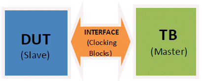
Figure 1: Connecting the DUT and TB
DESCRIPTION OF THE INTERFACE WITH CLOCKING BLOCKS

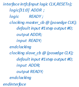
The Interface(intfc) provides the definition of two clocking blocks(master_cb and slave_cb) each consisting of clocking signals(ADDR and READY). In a multiple-environment scenario, definition of two clocking blocks (master_cb and slave_cb) will be required in the same interface(intfc) as both Master and Slave can act as a testbench for integration with different DUTs. In this article, considering a single environment scenario, Master will act as a TB and will refer the clocking block(master_cb).For every clocking signal defined in the clocking block, a corresponding clockvar is implicitely maintained by the clocking block itself.
DESCRIPTION OF THE DUT (SLAVE):

The module based DUT(slave_dut) samples CLK, RESETn and ADDR as inputs and drives READY as an output signal.
DESCRIPTION OF THE TESTBENCH (MASTER):

As mentioned above, the clocking block (master_cb) is being used by the Testbench(Master) for sampling READY as input and driving ADDR as an output.
The TB samples and drives the clockvars which are associated with the input(READY) and output(ADDR) clocking signals of the clocking block(master_cb) respectively.
DESCRIPTION OF THE TOP MODULE:

The top-module instantiates the DUT(slave_dut) and the Testbench(master_test). The interface signals have been port-mapped individually with the DUT signals.
DESCRIPTION OF THE ERROR/WARNING MESSAGES RECEIVED DURING SIMULATION ACROSS DIFFERENT SIMULATORS.
The Error/Warning messages across different simulators reveal that the interface signal ‘READY’ is written by procedural and continuous assignments.
The LRM section 14.16.2 Driving clocking output signals (IEEE Std 1800-2009) says that :- “It shall be illegal to write to a variable with a continuous assignment, a procedural continuous assignment, or a primitive when that variable is associated with an output clockvar”.
It implies that when an interface signal is declared as an output in any of the clocking blocks defined in the interface, than an implicit procedural assignment happens on that signal by the output clockvar associated with that signal.
However, in the example given above, during instantiation of the module (slave_dut), the interface signal READY is being mapped with the DUT in the following manner:

Port-mapping interface signal READY with the DUT in a way shown above is violating the SV LRM section 14.16.2 since READY, also declared as an output in the ‘slave_cb’ clocking block, is getting driven continuously. Since, procedural and continuous assignments are happening on READY at the same time, it resulted in a multiple driver scenario.
FIXING THE MULTIPLE DRIVER ERROR/WARNING MESSAGES USING WRAPPER INTERFACES
Preventing the creation of multiple drivers in such scenarios can be facilitated by using the ‘Wrapper Interface’. A Wrapper Interface is not going to contain the definition of clocking blocks and will serve as a medium to connect the DUT and the TB.

DESCRIPTION OF WRAPPER INTERFACE:

The above wrapper interface defines all the signals which are present in the main interface but will not specify any of these signals inside the clocking blocks.
DESCRIPTION OF WRAPPER MODULE:

The Wrapper module procedurally assigns the value of DUT’s READY to the main-interface’s (containing the clocking blocks) READY via the Wrapper Interface. So, only procedural assignment is happening on main-interface’s READY at a time.
DESCRIPTION OF THE TOP MODULE:

The top-module instantiates the DUT(slave_dut) and the Testbench(master_test). Besides the DUT and Testbench instantiation, wrapper interface and wrapper module have also been instantiated. The Wrapper Interface signals have been port-mapped individually with the DUT signals. Since, the wrapper interface(which doesn’t contain any clocking blocks)signals have been used to port map with DUT signals, multiple drivers are not created.
CONCLUSION :
A Verification environment in which the interface definition provides the declaration of multiple clocking blocks, so as to facilitate the usage of different components as testbenches, should define wrapper interface to prevent the creation of multiple drivers while integrating a DUT and TB.
