Nalin Gupta & Gaurav Goya (NXP Semiconductor, India)
As IC’s become more and more complex in the modern era, the challenges in meeting all the design requirements have become increasingly difficult. Some of the challenges applicable to all the SoC’s are High-performance, Low-power with reduced Die size.
Among all these challenges, hold timing closure is also one of the biggest challenges in front of designers right now as:
- A hold failure at silicon is very risky. Setup failure still can be managed.
- Lack of visibility of hold timing before skew introduction stage.
- By the time design is at skew introduction stage, design gets saturated in terms ofpower/area/routing resources & a lot of congestion has been seen due to Hold fixing.
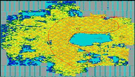
To consider the below snapshot from a design, which is a post skew introduction stage shows highly dense region as highlighted in Red outline. Any hold element addition(adds delay) for HOLD fixing in such regions is near to impossible or if done huge congestion can be seen for sure.

Fig. 1: A typical design shows highly dense region.
Generally, Hold timing closure can be achieved by any of the following below techniques which gets used depending on the magnitude of hold violations:
a) Routing:
It helps to reduce the hold violations either by lengthening of the wire routes or by hopping it into more resistance layers/slower metal layers. Generally this is effective to cater the hold violations which are of less magnitude and saves hold elements addition which further saves area/power.
b) Combinational Hold elements:
Generally a hold fix is achieved with the usage of buffers in the path which inserts the delay & fixes hold.
There are further two categories to it:
- Buffer cells: Buffers which are chosen to fix hold are of low drive strength cells so as to provide large delay. Doing this would result in less number of buffer usages. To fix smaller magnitude of hold violations, such low drive strength buffer cells are efficient to use which would consume less area/power and helps in improving the QoR of the design.
- Delay cells: There is another category of special buffers called as Delay cells which generally are used to fix hold with huge magnitude of violations. Delay cells have the same functionality as that of a buffer but with larger delay, larger area and high power. To fix larger magnitude of hold violations, delay cells are efficient to use which would consume less area/power and helps in improving the QoR of the design which otherwise would be fixed by the usage of huge buffers. Also, it is practically not possible to put chain of 30 buffers in the highly dense region as shown in the Fig. 1 while delay cell can do the job easily for the same delay requirements. Such scenarios can be benefitted with the use of delay cells.
There exist several architectures of delay cells:
2.a) Architecture based on channel length variation:
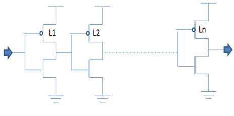
Below Fig. 2 architecture is based upon the usage of different and larger channel lengths for MOS devices within a single delay cell so as to provide more delay. Channel lengths can be larger than the technology node’s gate length defined. In this architecture since the gate/channel lengths have been used are not same & non-uniform which results in unpredictability of delay variations on the silicon. To use such delay cells there is a need to have more margins taken in the design to counter such unpredictability of the delay variation. Different gate lengths can lead to variations in different directions.

Fig. 2 Delay architecture with usage of different channel lengths MOS devices (L1, L2, . . Ln)
Such delay cell consumes less area and provides higher delay which would benefit the design.
2.b) Architecture based on stacking of MOS devices:
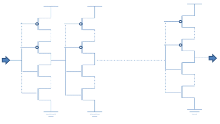
Below Fig. 3 architecture of delay cell is based on the usage of same channel lengths throughout the cell architecture but for larger delays stacking of MOS devices has been used. Doing this would increase the layout area but predictability in delay variations is there.

Fig. 3 Delay architecture with usage of same channel length with stacking of MOS devices.
Such delay cell consumes more area and provides higher delay which would benefit the design by having the need of minimum design margins.
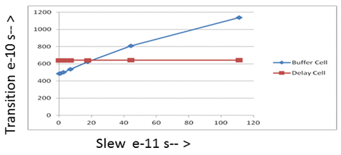
Typically, any delay cell is used to provide a particular delay and also expected to give as minimum variation as possible when used under different environments. Delay cells when used across different environments as compared to other normal cells provided in the library have less variation as compared to other normal cells as shown in the Fig.4.

Fig.4: Transition variations for Delay cell and Buffer cell across slews for a given load
c) Sequential Hold element:
There is also another class of hold fixing Flip-Flops which are hold friendly. Using this can be a boon in congestion critical regions but it can only provide the delay somewhere between a normal buffer cell and delay cells.
Conclusions and Future Directions:
As discussed above, it can be inferred that depending on the magnitude of the hold violations, techniques can be classified as efficient for that magnitude or not while it highly depends upon the design to design and can be changed accordingly.
Below are the acronyms which are used above.
| Acronym | Explanation |
| SoC | System on Chip |
| PD Flow | Physical Design Flow |
| PVT | Process Voltage Temperature |
| QoR | Quality of Results |
| MOS | Metal Oxide Semiconductor |
