By Frederick Kalinian/Gordon Harling (Innotime Technologies Inc.) , Hugh Pollitt-Smith (CMC Microsystems)
Abstract—The market for Semiconductor Intellectual Property is well served for standard process technologies but not all functions are offered in all processes. Mixing and matching high performance digital CMOS, analog components, MEMS and optical devices can be an expensive and risky endeavour. Users often want to create a functional prototype for testing and sampling before committing to full production tooling or custom process development. Silicon Interposers can fill the gap by allowing users to mix and match components in different fabrication technologies with numerous advantages over Printed Circuit Board implementations.
Index Terms—Silicon Interposers, Prototyping, Hardware, Through Silicon Vias, TSVs
INTRODUCTION
Silicon Interposers are substrates with signal pass-throughs made possible by Through-Silicon-Vias (TSVs). Metallization on either side of the interposer can be used to provide interconnect between mounted components, including passives, but the bottom side interconnect can also be used as Under-Ball-Metallization (UBM) to transform the interposer into a surface-mountable module in a larger system. The TSV connections from top to bottom of the interposer make it a versatile and efficient packaging system.
Silicon interposers have a variety of advantages over printed Circuit Board (PCB) implementations including improved size, speed, power, excellent rigidity, good thermal matching to silicon components, minimal outgassing or contamination in extreme environments, well-controlled RF performance, and excellent reliability.
INTERPOSER IMPLEMENTATION
Innotime has designed a simple, regular base array of TSVs with common spacing and size. The base arrays are purchased from multiple sources and are inventoried to reduce customization cycle time. Base array wafers are held in inventory prior to patterning of the top side and bottom side metallization so that prototypes can be completed rapidly in a few mask steps. This approach reduces cycle time for new designs and offers a range of wafer size and TSV performance at reasonable cost.
The customized routing can be carried out at various laboratories and customers can choose a compatible supplier. Suppliers often have different equipment capabilities and research interests so it is up to the customer to choose a suitable supplier.
The design kit is available in the Tanner tool suite but data conversion from PCB tools is also possible.

Figure 1: Silicon Interposer Side View
Metallization for these devices can be performed in multiple laboratories across Canada. To ensure accurate simulation and consistent results each potential supplier is asked to fabricate a test chip design which validates the basic characteristics of various layers and structures. Beyond the basic design kit each laboratory offers specialized services and equipment for modifications to the base design in accordance with their particular expertise and focus; areas of special interest are electro-optics, sensors, biomedical devices, energy harvesting, and nanomaterials.
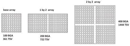
The base arrays for the interposer design contain 361 TSVs in a 19 by 19 array and are surrounded by a scribe channel. Users may define square or rectangular areas depending on the desired size of their design as shown in Figure 2 below. This allows for a range of product sizes and the possibility of using multi-project wafers to reduce costs. Standard package designs are available for the various configurations of tiles up to 2 by 2.

Figure 2: Silicon Interposer Tile Formats
INTERPOSER ADVANTAGES
Interposers allow the user to implement a design rapidly using off the shelf components for early measurement, field testing or sampling. Some of the specific advantages are:
- Size – At least 10 X reduction in size versus PCB implementation, linewidths and spaces in the basic implementation are 5 micron/5 micron versus 75 micron/75 micron for a PCB board using 3 mil lines and spaces. Bare die and chip-scale packages can be bumped and flip-chip mounted or wire-bonded without the area penalty of package leads.
- Performance – Interconnect is formed using tightly controlled semiconductor technology so fabrication variation is minimized. RF performance is improved by the reduction of parasitic components using flip-chip technology and avoiding package pins and wire-bonds where possible.
- Power - reduction of parasitic components and the need to use high power drivers to drive pins.
- Reusable IP – Schematics and layouts for various common blocks are offered as part of the Physical Design Kit in the Tanner tool suite. This can simplify and reduce risk related to customer implementation of blocks such as energy harvesting, RF communications, power monitoring or other common sub-functions. By taking a ‘crowd-sourcing’ approach to the development of common blocks we expect to create a large library of component footprints, reference design blocks and simple functions to aid in ‘cutting and pasting’ an interposer design..
- Rapid prototyping is available since the pre-processed TSV substrates are kept in stock and only a small number of metallization and component placement steps are required to complete samples.
- In some applications, such as in high vacuum detectors, the use of organics is prescribed due to outgassing concerns. Silicon Interposers are a quick and easy replacement using the same design files as a PCB implementation.
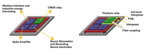
Figure 3 below shows two simple examples of designs implemented using interposers. On the left is a biomedical device with energy harvesting and a wireless interface while on the right is an electro-optical design which features an interposer daughterboard for more complex routing. The underside of the device may be used simply for routing, in the case of an independent module, or it may be populated with a Ball Grid Array using a standard pre-defined pitch.

Figure 3: Sample Interposer Reference Designs
A CANADIAN ECOSYSTEM FOR RAPID PROTOTYPING
This initiative arises from Embedded Systems Canada (emSYSCAN), a pan-Canadian project involving researchers at 37 institutions and featuring rapid prototyping as a key theme. The silicon interposer technology integrates with other aspects of the emSYSCAN project, including design environments for constituent technologies (e.g., CMOS, GaN, MEMS, Silicon Photonics) and for the interconnect on the interposer itself, as well as programmable system demonstrators (FPGA-based) for embedded software development and system validation. This infrastructure aligns with complementary products and services available to researchers through CMC Microsystems as part of Canada’s National Design Network: component manufacturing, packaging and fixturing, test and characterization equipment, and access to university micro/nano-technology (MNT) laboratories. These capabilities combined describe a comprehensive ecosystem for embedded micro/nano-systems rapid prototyping and demonstration.
CONCLUSIONS
Silicon interposers using a base array approach can be a useful tool for implementing microelectronic systems based on heterogeneous or incompatible technologies. They can offer a rapid path to a product which can be field tested and sampled prior to full SoC integration. They have numerous advantages over PCB implementations and costs can be very competitive.
ACKNOWLEDGMENTS
This work was carried out under contract to Queen’s University and CMC Microsystems as part of the Embedded Systems Canada (emSYSCAN) project funded by the Canada Foundation for Innovation (CFI) and participating provinces.
Many thanks to SoftMEMS and to Spark Microsystems for work on the design kit as well as the many FabLabs across Canada who have participated in this development.
REFERENCES
F. Kalinian, G. Harling, H. Pollitt-Smith, “Multitechnology Interposer Specification” Publically Available Internal Document, August 2016.
