Sreenath Panganamala, Nishith Sharma, Sriram Balasubramanian (Synopsys)
Abstract:
The paper discusses about Execute In Place (XiP) feature in embedded systems implemented through the SPI protocol. Concept of XiP are explained including how it improves the overall throughput and efficiency of a system. Results are shared on the overall system throughput improvement. Further we discuss about various methods by which user can make most out of this feature.
Keywords:
Execute In Place, NOR Flash, SPI
I. INTRODUCTION
NOR flash memories have been popularly used in embedded devices for very long time due to their reliable data storage. For some of the low-power applications serial NOR is becoming more popular than parallel NOR flash devices. Parallel NOR flash gives higher throughput in comparison to serial NOR due to its parallel nature. But with the emergence of multi-lane (2-8 parallel data lines) support in serial NOR devices, it has now become more popular for low power devices. These flash devices are mainly used in embedded system to store boot code and sometimes as storage elements. These boot devices uses the Execute in place (here on referred as XIP) method to execute the code from the native memory device. The XIP approach contrasts an approach where the code is first moved from its starting location prior to execution. An XIP approach typically reduces the number of memory components required and improves startup time, since code need not be moved prior to execution. New innovations in SPI devices, like octal transfer format and DDR operations, enable them to be used at very high speeds and improving the performance of system. This paper describes both system level and memory device strategies that could be used to exploit the XIP feature provided by memory devices.
II. SERIAL VS PARALLEL NOR DEVICES
There are two primary types of NOR devices: serial and parallel. Serial NOR provides access over a small pin-count serial interface such as SPI. These devices are targeted at cost and size constrained applications due to their low pin counts and resulting small package sizes. While Parallel NOR devices have a much wider interface and thus have much higher performance, but require larger packages and generally higher costs than serial devices. That’s why Serial NOR devices are typically found in space and power constrained designs such as handheld equipment, meters, sensors, set-top boxes (STBs), printers, local routers, and hard disk drives. The XIP performance of parallel NOR devices is much better than serial NOR, but due to its low cost and power serial NOR devices has become more popular in embedded systems. With parallel NOR typical bandwidth one can get is 250 MBps on 133 MHz clock and for the serial NOR typical speed is 54 MBps with 108MHz clock. [1]
III. SERIAL NOR DEVICES
Serial NOR devices use protocols like I2C, Microwire and SPI to interface with memories. All these protocols use one/two data lines to interface with the device. Recent enhancements in SPI protocol, like introduction of Dual, Quad and Octal mode and capability to perform DDR operations, have made SPI a preferable option to be used with higher throughput. SPI was initially a three-wire protocol consisting of two data lines and one clock line, but due to the higher demands for throughputs in embedded devices new multi-lane protocols have been introduced by various vendors to improve the performance of the device.
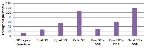
With recent improvements, Dual data rate protocol has also been introduced in SPI devices which have pushed further boundaries in throughput. Figure 1 shows the throughput for various flavors of SPI devices with SDR operation frequency of 108 MHz and DDR frequency of 133 MHz. New SPI devices are coming up in market which provides up to 133 MHz frequency support in SDR and 80 MHz support in DDR mode which results in throughput of 133MBps and 160MBps respectively. These innovations have significantly closed the gap between parallel and NOR flash devices providing a low-cost solution for higher throughput requirement systems.
IV. EXECUTE IN PLACE
An Embedded system typically contains one off chip NOR Flash which is interfaced using an SPI peripheral. The boot code is stored in NOR flash device and it is executed by moving it to a RAM. This process is time consuming and requires additional hardware in the system in terms of memory device.
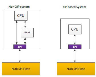
Execute in place approach removes the need of extra RAM inside the device (described in Figure 2). The code is directly executed from Non-volatile memory and not moved into local storage for the execution. This improves the efficiency of system as well as reduces the area. Since the code is directly executed from the memory it improves the performance of device as well.

Figure 1 Throughput comparison of various SPI flavors

Figure 2 XIP vs. Non- XIP system
V. INTERFACING WITH SERIAL NOR
SPI serial NOR devices uses host controller to interface with devices. A typical process includes process explained in Figure 3.

Figure 3 Interfacing with SPI device via controller
This process does not take the full advantage of the SPI throughput and end up being very slow. For fetching 16 Bytes of data from the Octal SPI memory running on 108 MHz frequency, following delays are involved:
| Process | Time (in SPI clock cycles) |
| Programming the Controller | 4 |
| Controller latency | 8 |
| Instruction transmit | 8 |
| Address Transmit | 3 |
| Data Receive time | 16 |
| Data fetch from the controller | 8 |
So a total of 43 clock cycles are required to receive 16 bytes of data, which results in overall throughput of 20 MBps.
Therefore we are only able to use 37% of throughput from the device. – (i)
Execute in place feature removes the controller latency and converts the controller into a memory mapped interface. This lets user execute the code on NOR flash memories in place and hence called Execute in Place mode. XIP commands in SPI devices remove the need for instruction to be sent for each data transmission, this improves the overall throughput and the controller can be enhanced to be used as a memory mapped I/O for SPI device. In similar scenario as explained above the throughput calculations are updated as below:
| Process | Time (in SPI clock cycles) |
| Controller latency | 4 |
| Address Transmit | 3 |
| Data Receive time | 16 |
So it takes a total of 23 clock cycles to transmit 16 bytes of data resulting in overall throughput of 55 MBps. – (ii)
By this mechanism we can use 50% of throughput from the device, an improvement of 20% as compared to the legacy use model.
VI. IMPROVING THROUGHPUT VIA EXECUTE IN PLACE
Ever since the introduction of Execute in place memories, SPI has become very popular for low power solutions. There are many innovations done by memory devices to reduce boot time of device like removal of address phase from the XIP transfers. These improvements have decreased the memory access time significantly. Still the overall throughput utilization is less for the device. Still there are some techniques that can be utilized to improve the throughput further, following sections discusses such techniques.
A. USE LARGER BLOCK SIZE
Another way in which user can improve the performance further is by increasing the block size of device. For example, if we want to fetch 1 KB of data from memory there are two ways in which it can be done.
Case 1: data is read in chunks of 16 Bytes
This leaves us the overall throughput of 55 MBps
As calculated in result (ii).
Case 2: All the data is read out by one command
| Process | Time (in SPI clock cycles) |
| Controller latency | 4 |
| Address Transmit | 3 |
| Data Receive time | 1024 |
So it takes 1031 clock cycles to receive 1KB of data.
So, overall throughput comes out to be 107MBps – (iii)
This is close to 99% of overall bandwidth. So by fetching a larger chunk of data from memory we can reach close to 99% of the device. In this method the data is pipelined utilizing the complete bandwidth of the device.
B. DATA STORAGE IN CONTIGOUS LOCATIONS
Mostly the data stored on the NOR flash devices in embedded system contains the boot code which is read-only. The data could be organized in such a way that it can be fetched in one single command. If the code has many jumps in between then CPU must send the address again to read from that location and this in turn can reduce the overall bandwidth. Let’s consider a case where we have 1 KB of code which is stored in contiguous location, the throughput to fetch that data in one command would be 107MBps at 108 MHz of clock as calculated in result iii.
Now consider a case where we have 40 Jumps in the data stream then it would require us to send 40 addresses again and additional controller (typical value) latency for each jump.
| Process | Time (in SPI clock cycles) |
| Controller latency | 4 * 40 |
| Address Transmit | 3 * 40 |
| Data Receive time | 1024 |
Total time to receive 1024 bytes of data is 1304 clocks. So the overall throughput of 85MBps – (iv)
This is around 78% of maximum throughput.
As observed, changing the organization of data has a big effect on the overall XIP performance.
VII. RESULTS
Following are results after incorporating Execute in place method and further improvements by introducing new implementation techniques
| Method | Overall Throughput (in MBps) | Utilization |
| Interfacing with SPI controller | 20 | 37% |
| Using Execute in Place method | 55 | 50 |
| Using Larger block size for data fetch | 107 | 99% |
| Using lots of branch functions in boot code | 85 | 78% |
As observed, introducing Execute In Place technique for code execution increases the overall performance of device significantly and provide best low power solution for embedded systems. Further the bandwidth utilization can be improved by improving the code organization and increasing the block size for the code fetch.
VIII. CONCLUSION
With the newer devices coming up in the market with better speed and new transfer formats, the throughput achievable by SPI Serial NOR memories have come very close to parallel NOR devices. With addition of XIP feature, the serial NOR has now become favorite option for embedded and low power systems. To make most out of XIP functionality one can improve how the data is saved in flash and increase the overall throughput and some software enhancements can be done to remove address and wait cycles from the transfer. In the coming years, more enhancements are expected in Serial NOR devices which will increase the throughput further and consuming low power.
The DesignWare SSI IP from Synopsys supports the complete various XIP modes featured in this paper and provides a high performance, low power and low area solution to the market. The availability of APB/AHB interface provides flexibility for customers to choose the right solution based the performance need and application.
VIII. REFERENCES
[1] NAND flash guide by Micron
[2] Micron Serial NOR Flash Memory Part no. N25Q256A – data sheet
[3] Spansion Application note, S25FL-S AutoBoot Function, 2015
[4] Spansion Serial Peripheral Interface with Multi-I/O, Part no. S25FL128S and S25FL256S data book
[5] Winbond Serial Flash memory with Dual and Quad SPI, Part no. W25Q64BV data book
[6] Cliff Zitlow, Improved Memory Throughput Using Serial NOR Flash, White paper, 2012
[7] Jared Hulbert, Introducing the Advanced XIP File System, 2008
