Yoav Lavi, VLSI Plus
July 2017
In this article, we show how fast video streams conforming to MIPI CSI2 rev2.0 over MIPI DPHY rev1.2 can be generated, using VLSI Plus’ SVTPlus-CSI2-F IP core, with simple off-FPGA analog front-end. The high bit rates can be achieved with a relatively slow FPGA clock frequency, trading off FPGA resources for simple timing closure.

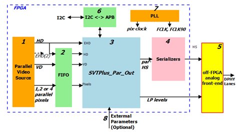
Figure 1: System Overview
System Overview
- A typical parallel video source is any parallel-output digital camera. 1,2 or 4 parallel pixels are input per clock cycle, along with HD, VD and EHD.
- An Early-HD (EHD) signal is needed, to initiate the generation of long packets. Many cameras have an internal indication prior to the start of the video stream, which can be used as EHD (for example, in image sensors – start column analog to digital conversion). In those cases, Delay Unit 2 will not be needed. When this is not the case, an optional Delay unit (FIFO) is added.
- The SVTPlus-Par-Out is the RTL part of the IP. DPHY lanes have two modes of operation – high-speed, in which each lane is a differential transmitter, and low-power, where each of the two wires of each lane assumes different CMOS levels, as defined by the protocol. The SVTPlus-Par-Out drives the low-power levels directly, and outputs parallel bytes for the high-speed mode, which are then serialized.
- For low bit rates, one can use an RTL serializer, which is provided with the IP. For higher bit rates, up to 2.5Gbps, one should use an FPGA specific I/O bound high-speed serializer.
- The serialized high-speed lanes, in differential LVDS pairs, and the low-power signals generated by the SVTPlus-par-out, are output from the FPGA to an Analog-Front-End unit, which then drives the DPHY lanes. The analog front end may be DPHY compliant, in which case it is implemented by active components such as the MC20902, or DPHY compatible, in which case passive components only are needed (but strict DPHY compliance is not provided).
- Operation is controlled and monitored by a set of AMBA-APB registers. An I2C2APB can be optionally added, for I2C access. Note that the CCI protocol defined in the CSI2 specifications is a subset of I2C, and it will be supported with this option.
- Bit rate at the parallel-video input and at the DPHY lanes output must match. This is obtained by generating two clocks – FCLK/FCLK90 for the lanes, and PIX-CLK for the input path. The frequency ratio FCLK/PIX-CLK must be equal to 2*PPC*BPP/Lanes, where PPC is the number of parallel pixels at the input (1,2 or 4), BPP is the number of bits per pixel and Lanes is the number of configured DPHY data lanes. The clocks are typically generated by a PLL in the FPGA.
- Some applications require multiplexing of several video sources, using CSI2 Virtual Channels and/or different data types. This can be done by reprogramming the video parameters in the SVTPlus-CSI2-F registers, but for more efficient multiplexing, the user may wish to use hardware multiplexing external to the IP. In this case, extra input pads are added for the parameters, and the corresponding registers are not implemented.
Frequencies
Data rate at the MIPI DPHY lanes, in bps, equals to L*bps, where L is the number of configured data lanes, and bps is the bit rate per lane. The internal SVTPlus data path is 64-bit wide, so that the maximum clock rate required is L*bps/64. With 8 lanes at 1.5Gbps per lane, the internal frequency will be 187.7MHz, and, at the theoretical maximum of 8 lanes and 2.5Gbps per lane, 312.5MHz will be required.
Let’s examine three examples. We assume that the gaps in the video transmission – inter-line and inter-frame – constitute 10% of the transmission time:
1. FHD
- 1920x1080 pixels per frame
- 60fps
- RAW12 (12 bits per pixel)
- Average bit-rate: 1920*1080*12*60 = 1.492Gbps
- Peak bit-rate: 1.492 * 1.1 = 1.64Gbps
- Peak input pixel rate: 1920*1080*60*1.1 = 136.9MHz
One or two data lanes will be required to handle this rate. The preferred input option (PPC) will be one-pixel-per-clock.
2. UHD (4K)
- 3840x2160 pixels per fame
- 60fp
- RAW14 (14 bits per pixel)
- Average bit rate – 3840*2160*60*14 = 6.97Gbps
- Peak bit rate – 6.97 * 1.1 = 7.66Gbps
- Peak input pixel rate – 3840*2160*60*1.1 = 547MHz
Four 1.92Gbps per lane or. for example, 6 1.25Gbps lanes are needed. 2PPC option is advisable, for 273.5MHz internal clock
3. FUHD (8K)
- 7680x4320 pixels per fame
- 30fp
- RAW16 or RGB565 (16 bits per pixel)
- Average bit rate – 7680*4320*30*16 = 15.93Gbps
- Peak bit rate – 15.93 * 1.1 = 17.52Gbps
- Peak input pixel rate – 7680*4320*30*1.1 = 1009MHz
Eight 2.2Gbps data lanes are required. 4PPC option is advisable, for252MHz operation
Serialization
The SVTPlus-CSI2-F IP core comprises two parts – the svtplus_csi2_par_out module and the serializers module.
Figure 2 depicts the serialization scheme. The svtplus_csi2_par_out module outputs lane data in bytes – hsb1 to hsbn, where n is the number of configured data lanes. The serializers module converts byte data to serial, and outputs high speed stream to the off-FPGA analog front-end, separately for each data lane.
A high-speed DDR clock (FCLK) is input to the serializers module, which divides it by 4 to generate the hsblk clock – the byte sampling clock.
The svtplus_csi2_par_out module, containing most of the SVTPlus-CSI2-F IP logic is provided in RTL form, and is FPGA independent.

Figure 2: Serializers
The serializers module is also provided in a RTL form, but RTL implementation is limited in performance (depends on the target FPGA), and cannot be used for high bit rates. Instead, the system implementer should replace the RTL serializers with IO bound FPGA-specific high speed serializers. High speed serializers are typically generated by a tool provided by the FPGA vendor.
Analog front-end
MIPI DPHY connection comprises one clock lane, and several data lanes (the number of data lanes was initially limited to four, but that limit was removed in later editions). Each lane comprises two wires and has two modes of operation - HS, in which the wires transfer differential high speed data at low voltage swing, and LP, where each of the two wires assumes CMOS logic levels according to some protocol, as detailed in the DPHY specifications. The sequence of LP levels in the two lanes is used to signal start and end of high speed packets, and to transfer escape-code messages.

Figure 3: Active Analog Front-End
In FPGA implementation of the DPHY, driving the lane wires is typically done by an analog front-end circuit, outside the FPGA.

Figure 4: Passive Analog Front End
Two main approaches are – using an active component (e.g. the MC20902) for a DPHY compliant solution (Figure 3), or using passive-component network (Figure 4), for a solution compatible with DPHY receivers, but not compliant with the DPHY specifications. This second solution is described in application notes of some of the leading FPGA vendors.
CCM and NCCM Modes
MIPI DPHY defines two modes of clock lane operation – continuous clock mode (CCM), where the clock lane is always active, and non-continuous clock mode (NCCM), where the clock lane assumes LP (Low-Power) state between packets. NCCM operation saves power, but, as the overhead for turning the clock lane on and off is significant, it reduces the transmission bandwidth.
The SVTPlus-CSI2-F has four modes of clock-lane operation:
- Programmed CCM (PCCM)
- Constant CCM (CCCM)
- Horizontal-Vertical-CLK-Stop (HVNCCM)
- Vertical-CLK-Stop (VNCCM)

Figure 5: PCCM Mode
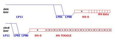
Figure 5 depicts the clock lane behavior in PCCM mode. Upon reset the clock lane is in LP00. When the IP is enabled (by writing 1 in its Enable register), the lane starts a timed sequence of LP11, LP01, HS0 and HS-toggle. The time duration for each stage is defined in the DPHY specifications. After the clock lane reaches HS-toggle, it toggles until it will be disabled or reset.
PCCM is the proper way to enter continuous clock mode. A compliant DPHY receiver has switchable termination resistor on the clock lane (as well as on all data lanes), and will connect the termination only after the clock lane is no longer in the LP01 state. However, there are some CCM DPHY receivers which expect continuous clock only, and do not have a termination on the clock lane. For those receivers, PCCM is not desirable, because during the LP01 state large current will flow through the termination resistor. For those receivers, the SVTPlus-CSI2-F offers the CCCM – constant CCM mode (Figure 6). When in this mode, the IP switched from LP00 to HS-toggle when it is enabled.

Figure 6: CCCM Mode
The overhead associated with turning the clock lane off and on is substantial. When a packet starts, the sequence which must be followed (see Figure 7) is:

Figure 7: NCCM Packet Start
- The clock lane goes to LP01
- The clock lane goes to LP00
- The clock lane transmits HS0
- the clock lane start toggling
- After 8 (or more) clock toggles, the data lanes go to LP01
- The data lanes go to LP00
- The data lanes transmit HS0
- The data lanes transmit the packet header, followed by the packet payload.
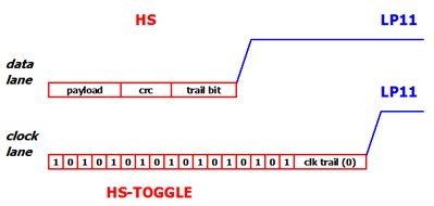
When a packet ends, the following (Figure 8) sequence takes place:

Figure 8: NCCM Packet End
- The data lanes send a packet footer – CRC
- The data lanes flip the last HS bit and transmit the flipped bit value (trail-bit)
- The data lanes transmit LP11
- The clock lane continues toggling for a specified time
- The clock lane transmits logic 0 at HS
- The clock lane switches to LP11
Each of the stages above has a minimum time specification. Overall, the overhead is quite substantial, and, as a result, NCCM has been popular only when low data rates are required, and the overhead is affordable.
There are applications where a single frame is too fast for NCCM, and yet frames are separated by long inactive periods, and keeping the clock lane active is undesirable.
With that in mind, the SVTPlus-CSI2-F IP has two modes of non-continuous-clock-mode (NCCM) – VNCCM and HVNCCM

Figure 9: HVNCCM
As depicted in Figure 9, in HVNCCM, the clock lane assumes LP11 between any two packets. The overhead, as shown above, is large, but power saving is maximal.

Figure 10: VNCCM
Figure 10 depicts the VNCCM mode. The clock lane enters LP11 only between frames. In applications where inter-frame gap is large and intra-frame gaps are small, this can be the optimal solution, saving power where it counts and avoiding NCCM overheads when speed is critical.
Timing Control
MIPI DPHY defines a multitude of timing parameters that the DPHY transmitter should comply with. Some of those parameters are defined in absolute ns units, some in UI (the time it takes to transmit one bit in one data lane) and others in combination of ns and UI.
Setting the timing parameters values far from the spec maximum or minimum is recommended whenever possible, but it may come at the cost of degraded performance.
The SVTPlus-CSI2-F has timing configuration registers which define 11 DPHY timing parameters, in pix-clk units. An easy-to-use spreadsheet programmer guide is provided with the IP, allowing user-controlled optimization of the various timing parameters. The spreadsheet lists the configuration values, and generates a script to program the registers.
Lane Calibration
MIPI CSI2 defines special calibration packets to adjust for inter-lane skew. Two types of calibration packets are defined – initial calibration, typically sent upon system powerup, and periodic calibration, typically sent every preset number of video frames. Initial calibration packet is longer than the periodic calibration packet.
The SVTPlus-CSI2-F supports both initial and periodic calibration. Two registers – ICR and PCR define the lengths of the Initial and Periodic calibration packets, respectively. An Initial Calibration Packet is sent whenever the ICR register is written into. Periodic Calibration packet is sent when a pulse in asserted on the Periodic-Calibration-Trigger pad of the SVTPlus-CSI2-F.
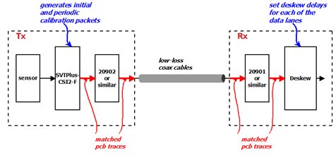
An interesting application of the calibration packets may be to increase the range of CSI2 over DPHY to several meters, as illustrated in Figure 11.

Figure 11: Long Range
Skew between the data lanes comprises mismatch in PCB traces, coax connectors and coax cables. The SVTPlus-CSI2-F generates initial and periodic calibration packets, which are detected in a Deskew circuit (typically a part of a DPHY Rx circuit) located in the Rx board. The Deskew circuit measures the inter-lane delays during calibration, and sets delay intervals for each of the data lanes accordingly. The delays are applied when video frames are received. This way the delays measured during calibration are compensated for, and long-range transmission can be achieved.
Customized video-format support
CSI2 rev 2.0 defines many video formats; only a few of them are mandatory. Some of the formats require a large amount of FPGA resources, which will be a waste for most application, but all video formats may be used.
To solve this dilemma, the SVTPlus-CSI2-F offers all CSI2 rev 2.0 video formats on a per-user customization basis, except for very few formats which are always provided. This is detailed in Table 1.
| Video format | CSI2 Coding | |
| RAW6 | 28 | customization |
| RAW7 | 29 | customization |
| RAW8 | 2A | standard |
| RAW10 | 2B | customization |
| RAW12 | 2C | customization |
| RAW14 | 2D | customization |
| RAW16 | 2E | standard |
| RAW20 | 2F | customization |
| RGB444 | 20 | customization |
| RGB555 | 21 | customization |
| RGB565 | 22 | standard |
| RGB666 | 23 | customization |
| RGB888 | 24 | customization |
| YUV420-8bit | 18,1C | standard |
| YUV420-10bit | 19,1D | customization |
| Legacy YUV420-8bit | 1A | standard |
| YUV422-8bit | 1E | standard |
| YUV422-10bit | 1F | customization |
| Generic 8-bit Long Packet | 10 to 17 | standard |
Table 1: Standard and Customized Video Formats
Likewise, implementation of video compression, which is seldom used, is offered as a customization option.
Multiplexing several video sources
One of the SVTPlus-CSI2-F options is External Parameters. When this option is selected. some of the CSI2 configuration bits, which are usually stored in registers, are input from external pads. The parameters are:
- FS-VC – the 2-bit virtual channel field of the Frame-Start short packet
- FE-VC – the 2-bit virtual channel field of the Frame-End short packet
- Frame-Count – the 16-bit frame-count field of the FS and FE short packets
- LP-header – the 24 bits of the Long-Packet header, including the 6-bit data-type field, the 2-bit Virtual Channel filed, and the 16-bit Word-Count field (indicating the length of the packet)
This option opens the way to a multitude of multiplexed-video applications, using simple off-IP logic.
Here are some examples:
1. Adding blank lines. A sensor sends blanking data in the first 10 lines of each frame, and it is required that DT field of the long packet header will be set to 0x11 (Blanking Data). In all other lines, the data type is 0x2C (RAW12).

Figure 12: External Parameters - Example 1
Figure 12 depicts the implementation of example-1. The off-IP circuit comprises a counter which keeps track of the current line; a comparator detecting the blanking lines, and a multiplexer which selects a DT value of 0x11 for the blanking lines, and 0x2C in all other lines.
2. Enhanced Dynamic Range application. In this example, a camera changes the exposure time of successive frames in a sequence of long, medium and short exposures. The receiver then builds a high dynamic range image from the three exposures. It is defined that the long exposure frame will be sent on virtual channel 0, the medium exposure frame on virtual channel 1 and the short exposure on virtual channel 2.

Figure 13: External Parameters - Example 2
Figure 13 illustrates how this configuration is implemented. The VC fields are input separately for Frame-Start (FS), Frame-End (FE) short packets, and for the long packet. A simple decoder translating the selected exposure time to 2 bits is all that is needed for this application
3. Interleaved video can also be implemented using the external parameters option. However, buffering should be added, to delay packets from one video source when the SVT-CSI2-F is busy transmitting packets from the other video source.
Also, the VD input of the SVT-CSI2-F cannot be used. Instead, the GSP – Generic Short-Packet; and the GSP-Trigger inputs of the IP should be used to generate FS and FE packets.
Summary
We briefly touched on how the SVTPlus-CSI2-F can be used to generate CSI2 rev 2.0 over DPHY rev 1.2 video. For more information, the reader is encouraged to download the SVTPlus-CSI2-F product brief from our website - http://www.vlsiplus.com/ipPDFs/svtplus_csi2_f_pb.pdf. For further information including the data sheet, please write to ip_products@vlsiplus.com
