K Chaitanya, Arun Prasad Elango, Nivin Ninan George, Chandrashekar B U (Synopsys (India))
Abstract
With the evolution of Internet of Things, the requirement for ultra-low power systems have increased. To design a low power system, we must apply all the possible low power methods at each level of the system implementation. Currently, most of the systems are designed by integrating off-the-shelf Digital and Analog Intellectual Property (IP) blocks. In this paper, we focus on achieving lower power for existing IPs and the importance of architecture level clock gating and EDA Tool inserted clock gating.
Keywords—Low Power, Internet of Things, EDA, Clock Gating
I. INTRODUCTION
Internet of Things (IoT) is a new era of computing which encompasses technologies like machine to machine(M2M), machine to infrastructure, machine to environment, the Internet of Everything, the Internet of Intelligent Things and intelligent systems[1]. Many companies and research organizations have offered a wide range of projections about the potential impact of IoT on the Internet and the economy during the next five to ten years[2].
Since, most IoT applications are driven to provide cost effective solutions, the cost of the IoT products plays disproportionately important role in the market viability. Due to this, IoT system developers do not target newer evolving protocols or technology nodes. Most IoT applications use existing protocols such as USB, I2C, etc. and Ultra Low Power fabrication processes. Given that most IoT devices are battery powered, small power budgets are a strict design requirement. To this end, designers must take care of implementing low power strategies at every level of abstraction such as inter-chip communication, SOC micro-architecture and technology node. IP vendors are also updating their designs to meet the specific needs of the IoT market. Some of the popular low power approaches that have been in use for some time now are Clock Gating, Gate Level Power Optimization, Multi-VDD, Multi-VT, Power Gating (PG) and Adaptive Voltage Scaling[3]. Reducing dynamic power is a major design focus for specialized IoT optimized Ultra Low Power (ULP) fabrication processes.
Clock gating (CG) is a widely-used design technique for reducing the dynamic power consumption applied at both the front-end design phase and back-end design phase. As per a recent survey on CG [4], CG can broadly be implemented at register level or architecture level. With recent advancements in the EDA tools CG at the register level is handled more efficiently [4]. A design architect has to deploy CG at every possible opportunity at the architecture level based on the specific conditions unique to the design and usage.
Per Nikaein et.al [5], the traffic pattern between M2M in major of the IoT applications can be mainly modeled into three types: Periodic Update (PU), Event-Driven(ED) and Payload Exchange(PE). PU is used in non-realtime and event triggered at regular time pattern. Some of the examples of PU are smart meter readings such as cooking gas, electricity, and water. ED is used in real-time or non-real-time based on event monitoring. Some of the examples of ED are alarms, emergency alerts (health, climatic). PE is used in response to the previous PU or ED traffic. These traffic models give us a picture that most of the IoT applications doesn’t have continuous traffic all the time which enables the designers to think about using power saving methods efficiently at protocol level or architecture level.
Most architecture level or protocol level implementations based on standard connectivity protocols comprise of active states (with traffic, without traffic) and low power states. It is common to implement PG to save power during the protocol-defined low power states. But during active states with minimal or no traffic, we cannot use PG because latencies in switching off power & re-power often exceed the protocol timeouts for entry and exit. Therefore, to reduce the power during active state, we can only use clock gating at architectural level. This can be achieved based on the traffic pattern. For transfers which are carried out in bursts (non-periodic in nature), it is possible to enter low power state when there is no traffic and save power. But in the case of periodic transfers the device needs to remain in active state. When device is in active state in applications such as tracking/monitoring systems, traffic may not be present for the complete period. Clock gating can be used very effectively to save power in such cases when there is no traffic, when implemented prudently. In this approach, instead of relying on protocol specific low power states to do clock gating we define efficient ways to perform clock gating to specific blocks based on internal architecture.
When we consider USB2.0 protocol as an example, the protocol comprises of active states (with traffic, without traffic) and low power modes such as L1(Sleep)/L2 (Suspend). During low power modes, the USB subsystem (controller and Physical Layer (PHY)) can enter PG or CG depending on entry and exit duration. When USB subsystem is in active state, PHY power is 20-50 times controller power. Traditionally, effort has obviously been spent on reducing PHY active power. But, there is a fundamental limit beyond which it is not easy to reduce the PHY power during active traffic. Considerable effort has also been spent on reducing PHY power when controller/PHY subsystem is not functionally used in the system and during Suspend conditions. During Suspend (long duration of entry and exit) the amount of power consumed by the subsystem can be very low due to controller PG and PHY low power techniques. But many use-cases cannot make use of USB Suspend (L2) and moreover Operating System support for USB Suspend (L2) has been slow in becoming mature. The Transition time between active and suspend is often 100+ms in practice. When USB applications require much lesser response transition time than Suspend (L2), they take advantage of L1 (Sleep). During Sleep, it was observed that the PHY power can be reduced by more than 99% by appropriate choice of active/idle transition times. But the controller Sleep power is not significantly reduced with traditional clock gating. Controller has limited power saving capability due to the requirement to wake up fast from Sleep. Due to Sleep recovery timing requirements, the controller cannot PG. In practice, this means controller Sleep power is 10-20 times PHY Sleep power. The proposed clock gating method was employed to handle the power saving when there is no traffic and during low power modes like above scenarios.
This paper is ordered as follows: Different Clock Gating Methods are discussed in Section II. Active Clock Gating and other methods are proposed in Section III. The results are discussed in Section IV and finally, Section V concludes the paper.
II. CLOCK GATING METHODS
In this Section, we will be discussing about register level and architectural level clock gating that can be applied at IP level. The power saving at each level (register/architectural) is orthogonal to each other. Each method (register/architectural) will achieve minimum power consumption under certain conditions, when we incorporate both, we will have global minimum power dissipation for an IP. Due to this we will be discussing about some of the existing clock gating methods and their modification that can be applied to existing IPs to reduce dynamic power. First, we will be discussing about EDA Tool Inserted Clock Gating (register level) then the Architectural Clock Gating methods.
A. EDA Tool Inserted Clock Gating (TICG)
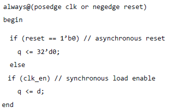
Currently, EDA tools provide clock gating options during synthesis. This is one of the efficient ways of inserting register level clock gating cells with minimal effort. The tool, based on the RTL coding style, detects the synchronous load-enable registers (flip-flops that share the same clock and synchronous control signals) and insert clock gating cells with synchronous control signals as enable condition to the corresponding clock. For the Design Compiler (DC) tool, the automatic insertion of CG is explained in [6] and [7]. For example, if the RTL is coded as below, DC checks the synchronous load enable signal clk_en in all the possible flops and then uses clk_en as one of the enable condition to gate the corresponding flops.
always@(posedge clk or negedge reset)
This method can be used for all the existing IPs. This method will provide optimal power saving to IPs which have a large register count. First, synthesize your IP and then analyze the register count, if you have a large register count you are likely to reduce large dynamic power provided you have synchronous load enable(s) in your design. Analyze the gated and ungated register report in the IP. If possible, check the ungated registers and see if there is a way to change your RTL coding style so that the tool can gate it. Manually estimate the power saved in your IP for gating certain registers by the tool. Compare that with changing all the ungated register into gated register. Following this method, we observed that in most of the cases the effort involved in changing the ungated register to gated register is high. In some of the case it will not be easy to modify coding style or some registers (CDC synchronizers) may not have synchronous load enables. Therefore, the power saving we get from the Tool Inserted Clock Gating(TICG) will not be completely optimal value but there can be further power reduction in all the cases.
B. Architectural Clock Gating
Architectural clock gating is mainly based on foreseeing which part of the design will be inactive under what condition and gate that part of the design accordingly. Architectural clock gating can evolve in two ways i) CG based on the protocol/design of the IP during implementation (Method1) ii) Analyze the design power after implementation and try to optimize the power using CG(Method2). In the latest literature survey [4], there are few architectural clock gating methods that can be useful for existing IP and if modification possible to them at IP level.
Chang et al. in [8] presented the Programmable Clock Gating (PCG) via a user programmable control register that determines the entry and exit of CG. This method will be useful if the exit and entry duration is high (considering the software latency). An effective implementation of PCG for DWC_mshc was shown in [9]. The disadvantage to this method is while disabling the clock gating, if the software latency is very high, it may lead to functional errors. A modification to the method is to use software for entry and exit with the help of additional wakeup logic. A further modification is providing a control register bit just to enable CG for safety purpose and logic for entry and exit.
Adaptive Clock Gating in another implementation which can be applied if complete IP can be modeled into a single Finite State Machine (FSM) with several states which can be divided into Working states and Idle states. In this method, we can gate the clock to the complete IP during idle states. Here there are no architecturally defined FSMs. This method was used for a Floating Point ALU which has several pipelines. When there are no instructions in the bus it was used for gating the clock assuming it is in one of the idle state of the IP. In most of the IPs based on standard protocols, the protocol itself defines the idle states for low power mode. Moreover, this method can be helpful for IPs having single clock domain. Nowadays most of the IPs have multiple clock domains, when an IP has multiple clock domains there will be scenarios were one clock domain will be inactive but the other domain will be active. In those cases, it is not easy to gate the clock with above method.
In Section III, we will be discussing the Active Clock Gating method which can be used to gate the clock in multiple clock domains environment.
III. PROPOSED CLOCK GATING METHODS
Active Clock Gating (ACG) is halting of active clocks in specific or major portions of the design based on the non-functional states of individual blocks of the IP.
Active clock gating is based on the following concepts:
1) If an FSM is in non-functional states then the logic related to that part of design is inactive.
2) If all the FSMs in a clock domain are in non-functional states then the logic in that domain is inactive.
3) If all the clock domain FSMs in an IP are in non-functional states then complete IP is inactive.
Consider an IP with N FSMs and M clock domains, ACG will be implemented as follows
- Generate an idle signal (idle_f1,idle_f2,…idle_fN) from each of the N FSMs in the IP when they are in non-functional states.
- Generate the wakeup signals (wakeup_c1,wakeup_c2,…wakeup_cM) from M clock domains which initiate the events in the domain.
- Generate idle signals (idle_c1,idle_c2,…idle_cM) for M clock domains by combining (AND) all idle signals and wake up siganls corresponding each clock domain.
- Synchronize the idle signals from each clock domain (idle_cs[2:M],idle_cs[3:M,1],…idle_cs[1:M-1) to other relevant clock domains they communicate to.
- Generate the clock gating enable signal (enable_c1,enable_c2,…enable_cM) for M clock domains by combining (AND) all idle signals and synchronized idle signals.
When we are trying to implement ACG for an existing IP first identify the existing FSMs in the design. Analyze the non-functional states in each FSM and the possible part of the design blocks which must be active even if the FSM is inactive. Most of these design blocks will be the wakeup or timers in the design triggering some of the events even if the FSMs are inactive. Clocks to this part of the design cannot be gated. Once we are clear on such blocks which must be ungated, provide an ungated clock to that part of the design. Generate the idle signals from each FSM and corresponding wakeup event related to that clock domain. When a FSM is in non-functional state this idle signal (idle_f[1:N]) will be high and in other states it will be low. When generating the wakeup signals in each clock domain there can be multiple wakeup events corresponding to each domain. Combine all the events wakeup to form a single clock domain wakeup (wakeup_c[1:M]) for each clock domain. When there is no wakeup event, the wakeup signal will be low and when there is a wakeup event the wakeup signal will be high. Combine all the idle signals and wakeup signals in a single clock domain to generate the domain idle signal idle_c[1:M]. This indicates that there are no functional events in the corresponding clock domain. The clock to this inactive domain can be gated but there can be events from the other active clock domains to the inactive clock domain which needs the clock to be active. To handle this, we can opt to keep clock active for all the synchronizers. But keeping in mind that there will be few synchronizers which trigger the wakeup events in inactive clock domain, only those wakeup synchronizers’ clock can be active and others can be gated if we can explicitly identify them in the design. This approach enables gating of one inactive clock domain even if the other clock domain is active. When considering the always active and wakeup events, protocol wakeup events due to remote incoming packets or application wakeup must be handled without violating protocol delays or causing functional issues. Once the always active and wakeup events are decided this method requires less effort and results in very effective dynamic power reduction for existing IPs.
The clock gating methods described above helps in identifying the domains which are inactive in a design during certain scenarios and gating them independently. But there can be other gating methods to interfaces such as Static Clock Gating and RAM Clock Gating. Static Clock Gating is gating the clock to the modules/interfaces which are inactive even when other interfaces are operational. The clock to those inactive interfaces can be gated.
IPs can use a single bigger RAM instead of using several separate small RAMs in the design. The clock to this RAM can be gated when there is no access to the RAM. RAMs support several levels of power savings based on content retention and recovery time after clock gating. This can also be used effectively to provide further power savings.
IV. RESULTS
We analyzed the amount of power saving due to different CG methods. The power was calculated using PrimeTime-PX tool on a Gate Level Netlist for a most popular 65nm low power node. The power saving techniques were implemented to an existing Synopsys USB IP. USB protocol already defines the active states (with traffic, without traffic) and low power states (L1/L2). In cases of L1(sleep), due to existence of smaller and continuous periods of minimum and no traffic durations, the controller cannot enter PG states. Traditional clock gating methods have not provided significant reduction in the power for IoT kind of applications. Therefore, to reduce the power during active state, ACG was used. For the same IP, power saving due to TICG was also analyzed. The IP configuration which we selected contained around 50% of combinational logic and 50% sequential logic. When tool inserted clock was employed, 75% of the registers were gated and 25% of them were ungated. Of the 25% ungated registers, 12.5% were related to synchronizers and always active registers which cannot be gated and other 12.5% contributed from registers for which there is a chance of gating. We analyzed all the functions of those 12.5% registers and if any register is amenable to gating, then modify it accordingly. It was easy in few cases but in most of the cases it was not easy to make them gated. With tool inserted clock gating having 75% of the registers gated there was a reduction in dynamic power by 58.27% as shown in Fig.1.
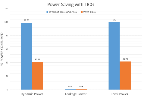
Fig. 1. Power Saving due to Tool Inserted Clock Gating (TICG)
The power saving when both clock domains were gated due to non-functional states was analyzed for ACG and there was a reduction in dynamic power by 84.30% as shown in Fig.2. The power saving when a single clock domain is inactive depends on the logic present in that clock domain. But sum of the power savings of individual clock domain is equal to the power saving when all clock domains are inactive.
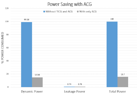
Fig. 2. Power Saving due to Active Clock Gating (ACG)
When both ACG and TICG was applied together to an existing IP there was a reduction in dynamic power around 91.09 % as shown in Fig.3.
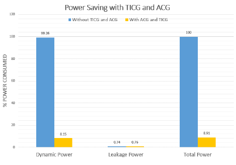
Fig. 3. Power Saving due to both ACG and TICG
Comparative power saving is shown in Fig. 4
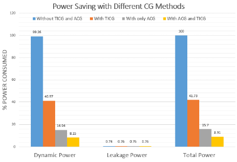
Fig. 4. Power Saving due to different CG methods
The power saving was measured for different technology nodes did not show much deviation implying that the technique does not depend on the technology node.
Table.1 shows the summary on percentage of power saving with TICG, ACG and both.
TABLE I. SUMMARY ON PERCENTAGE OF POWER SAVING
| CG Method | % of Power Saving |
| TICG | 58.27 |
| ACG | 84.30 |
| TICG and ACG | 91.09 |
V. CONCLUSION
In this work, we have discussed about PCG and its modifications which can be used for existing IPs. Clock gating techniques such as RAM Clock Gating and Static Clock Gating ideas were discussed. To a major extent, EDA Tool Inserted Clock Gating and Active Clock Gating require less effort but provide efficient dynamic power reduction for existing IPs. TICG provides optimal power saving without any additional manual effort, but to get the power saving to a minimal value more effort is needed. It is always better to use TICG for all IoT applications which have higher response latencies. Architectural level clock gating methods provide much higher power savings vis-à-vis effort spent in aggressively improving TICG percentage. Active clock gating techniques can be potentially extended to all design blocks. When implementing active clock gating, the implementer must ensure that protocol wakeup events due to remote incoming packets or application wakeup must be handled without violating protocol timeouts. The percentage of power saving due to ACG is invariant of technology nodes. From the results, it is evident that i) the amount of power saving due to ACG is much higher that the TICG during idle, ii) the amount of power saving increases when both ACG and TICG are used. Both methods complement each other and are applicable for multi-clock domain designs.
REFERENCES
[1] Karimi, Kaivan, and Gary Atkinson. "What the Internet of Things (IoT) needs to become a reality." White Paper, FreeScale and ARM (2013).
[2] Rose, K., S. Eldridge, and L. Chapin. "The Internet of Things (IoT): An Overview–Understanding the Issues and Challenges of a More Connected World." Internet Society (2015).
[3] Keating, Michael, et al. “Low power methodology manual: for system-on-chip design.” Springer Publishing Company, Incorporated, 2007.
[4] G. Pouiklis et al., "Clock Gating Methodologies and Tools: a Survey", Int'l Journal on Circuit Theory and Applications(2015).
[5] Nikaein, Navid; Laner, Markus; Zhou, Kaijie; Svoboda, Philipp; Drajic, Dejan; Popovic, Milica; Krco, Srdjan, "Simple Traffic Modeling Framework for Machine Type Communication, " Wireless Communication Systems (ISWCS 2013), Proceedings of the Tenth International Symposium on , vol., no., pp.1.5, 27-30(2013).
[6] Power Compiler User Guide, Version L-2016.03-SP4, Synopsys (2016).
[7] Mark Biegel Frank Emnett. “Power Reduction Through RTL Clock Gating”, SNUG, San Jose (2000).
[8] Xiaotao Chang, Mingming Zhang, Ge Zhang, Zhimin Zhang, and Jun Wang. “Adaptive Clock Gating Technique or Low Power IP Core in SoC Design.” In Circuits and Systems (ISCAS 2007). IEEE International Symposium on, pg 2120–2123, (May 2007).
[9] Harsharaj Ellur et al. “Achieving Ultra Low Power for Embedded Storage Application using Innovative Design Techniques”, Synopsys India Technical Conference (india) (2016)(Synopsys internal).
