by Navraj Nandra, Barcelona Design
Newark, California USA
Abstract :
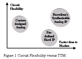
In this paper, we describe a new method of creating synthesizable full-custom analog intellectual property (IP) using geometric programming techniques. An engineer with little or no semiconductor design experience is able to configure the IP such that an optimally designed complex analog block can be obtained readily within hours. The rapid synthesis (or configuration) time allows an experienced designer to effectively perform system level design exploration and trade-off key constraints such as power, area and speed. The result of this new method is a tremendous increase in innovation and a radical acceleration of time to market compared to traditonal ways of obtaining analog IP as shown in Figure 1.
We present silicon tests results for analog IP blocks and detail the steps to create high performance PLL’s, that were required for a customer application using this new approach.
1. Introduction
The demand for analog IP is being driven by the high growth applications in the semiconductor market; where 10 years ago, industry shipments were dominated by PC and computer applications
that required digital, and by current standards, low frequency circuits, today consumer and communications applications dominate. Over the last five years, we have seen a consistent growth in the mixed-signal system-on-chip market. Technical advances in integrated circuit (IC) manufacturing processes have made it possible for true electronic systems[1], such as cameras and radio systems, to be integrated on a single silicon substrate. This emerging market is predicted to have very high growth rates in the order of 40% over the next five years. In 2005, it is expected that 65% of all SOCs will contain some analog components[2]. Since seven out of ten complex chips will contain analog, it means that there will be a fundamental shift from the way we design ICs today to the way we will design ICs in a few years from now. And this is leading to a shortage in supply because of the time needed to design the analog content on a mixed-signal SoC such as data converters and RF components. The percentage of SoC’s that require these types of circuits is correspondingly increasing from 20 to 70 percent over a ten year period. Further, almost all digital designs today require at least one phase lock loop for clock management ; the application of geometric programming techniques to the design of this essential building block will form the basis of proof in this paper.
Unfortunately, while this demand for analog has escalated, the supply, as mentioned above, has remained essentially flat, leading to a significant shortage. The number of analog designers is not increasing and neither is their productivity, as they use basically the same methods and tools as they have for many years.
The result is a major bottleneck.
Existing alternatives to the synthesizable full-custom analog IP method are presented in the following sections and their pros and cons. If specific requirements must be met, the available alternative is to create a custom design, either internally or with a design service provider. Such a design will take months, and as a trial and error process is the only available method, the schedule and results of such project can be uncertain. While this can result in a circuit that more closely matches requirements, it still lacks flexibility, as the analog circuit spec must still be set months before final tape-out.
2. Considerations for Successful Analog IP Deployment
There are several reasons that make analog circuit design in an SoC a very complex task. First of all, analog circuit performance depends on the transistor behavior. Small variations in the manufacturing process can result in dramatic changes in circuit performance. This translates into a need for accurate transistor models over different process corners. Another important concern in mixed-mode ICs is substrate noise coupling. Fast switching digital circuitry can deteriorate significantly the value of the sensitive analog signals. Also careful layout to reduce device mismatches and parasitics is crucial to guarantee correct circuit behavior. Finally, unlike digital circuits, the designer has to keep in mind a large number of performance specifications, making it time consuming to redesign an analog block.
Another important and overlooked issue is that an analog designer is required to create a new custom circuit or just perform new sizing of an already existing circuit. This design flow does not encapsulate the knowledge of this designer and as such it cannot be used later by a less experienced designer. For example, an experienced designer might know exactly what to tweak, change or be watchful of in a design. However, this information is not embedded anywhere so even if he has spent many months in a design, if he decides to leave the design group most of that information is lost.
The completely different design schedules of analog and digital was not an issue when two separate parts were sold. Semiconductor companies would market a new chipset every time a new IC process was released (even though only the digital part had changed). Today, however, in order to take advantage of the new process technologies, semiconductor companies are forced to have comparable design schedules for both analog and digital. This is a big issue because of the tremendous difference in design efficiency between the analog and digital parts. While the design of digital circuits is highly automated, the design of analog circuits is still manual.
Successful deployment of analog IP involves careful consideration of all the above items and these will be presented in the paper.
3. Options for Implementing Analog IP
Looking at this shortage more closely, semiconductor companies have two options for implementing analog circuits. Referring to Figure 1 again, they can source pre-defined hard IP either from an internal library group or a design service company offering fixed cells, or compilers based on fixed cells.
3.1 The Pre-Defined Hard IP option
This option offers a very small number of choices, making it unlikely that their requirements will be met, meaning the chip or system design must accomodate the specifications of the available cell. The vendors of analog IP however, face the same productivity problems in analog design; analog design takes so long that the off-the-shelf offering will be sparse. Thus this option is unlikely to offer a function that comes close to meeting the desired target specifications, compromising overall chip performance.
3.2 The Custom Designed Analog option
Alternatively, if specific requirements must be met, a custom design may be done, either internally or by an outside design consultant. Such a design can take months, and as a trial and error process is the only available method, the schedule and results of such project can be uncertain.
While this can result in a circuit that more closely matches requirements, it still lacks flexibility, as the analog circuit specification must still be set months before final tapeout. The designer begins with some sort of specifications for the circuit he needs to design. He starts by choosing a suitable architecture or topology.
After that, the next step is component sizing, in which the designer determines the sizes or values of the components for a given topology or architecture that achieve the requirements or specifications on the performance indices. Even though the numbers of design variables and performance constraints is often "small" by digital circuit design standards (say, a few tens or hundreds), this task can be very challenging, since in most cases all of the performance indices are affected by all of the design variables. Changing the length or width of just one transistor in an op-amp, say, will change all of the performance indices, sometimes by large amounts.
In order to reduce the design cycle time using the above mentioned approach, several commercial tools for the automation of the analog design process have become available on the market. These tools are best suited for design centering of circuit blocks. They are designed to increase the productivity of an already experienced circuit designer.
3.3 Attempts to Accelerate Custom Design Flow[3]
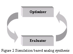
Figure 2 shows the approaches using simulation based analog synthesis. They have this overall structure. The loop is comprised of an optimizer proposing a candidate circuit and the evaluation engine, evaluating the quality of each candidate. And this keeps looping until the specification is met. The commerically available tools use SPICE and a numerical search engine or a bunch of numerical search engines. The optimizer can be :
• Simulated annealing
• Newton’s method
• Any other type of classical optimization methods
The method is CPU intensive and virtually impossible to handle a circuit with more than a few tens of transistors. Also, the method requires an analog designer AND and optimization expert: the experienced analog designer to input the SPICE deck and test benches; the optimization expert to select the step size, the search space and the search method.
It can take forever.
Component sizing is typically done in the following manner. Once the designer has calculated the device dimensions using first order equations he proceeds to use a simulator tool such as SPICE, which can determine the performance indices, given the design variables. The standard design approach is to repeatedly cycle through the following steps:
• Simulate the design to find the performance indices achieved• Think about how to change the design variables to improve the design
• Change the design variables
Attempts to automate this flow have consisted on letting a computer decide how to change the design variables, i.e., how to search the design space. The many methods differ on what engine is used.
The result of this set of poor choices, results in a severe limit on innovation; chip designs are limited by a limited number of circuit choices, and analog designers spend months on repetitive tasks like porting existing designs.
Barcelona’s approach breaks this bottleneck by providing synthesizable analog IP.
4. Synthesizable Analog IP
Using this approach designers can apply their own circuit specifications for a particular type of function, and generate a complete, custom-sized analog circuit in a matter of hours.
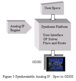
This approach offers much greater optimality and flexibility than even custom design, as there is no time constraint in finding the best sizing, and a chip design team can wait until late in the design process to finalize the analog function specs. The time-to-market is as good or better than off the shelf IP; Barcelona IP can be accessed just as fast as hard IP, and its flexibility helps with the overall TTM of the chip.
Importantly, this approach also yields a much more robust circuit, because ALL process, voltage and temperature conditions have been considered in synthesis.
4.1 Applying Geometric Programming to Analog
To put it another way : ‘What’s under the hood ?’
We observe that both transistor behavior and performance measures for analog IP blocks, such as phase locked loops and data converters, can be formulated as posynomial functions of the design variables. As a result, these design problems can be formulated as geometric programs, a special type of convex optimization problem for which very efficient global optimization methods have recently been developed. The synthesis method is therefore fast, and determines the globally optimal design; in particular the final solution is completely independent of the starting point (which can even be infeasible), and infeasible specifications are unambiguously detected. Methods to solve convex optimization problems have several advantages when compared to general-purpose optimization methods: they find the globally optimal solution; the solution can be computed extremely fast even for large problems; and, if a solution exists, convergence is guaranteed. Further details on geometric programming applied to analog design can be obtained from the following references : [4], [5], [6], and [7].
4.2 Introducing Miró – an Analog IP Engine
Because PLL's take a long time to design, are very prone to errors and extremely sensitive to noise, the solution is to build and test one or two PLL's that cover as many different applications as possible. When one works, and this was usually after one or two silicon re-spins, the same PLL, after a few tweaks, was used. However, this leads to sub-optimal designs and more importantly, as frequencies get higher and the jitter/noise rejection requirements become more challenging, this becomes a less and less viable option. The performance requirement is application specific which means a new PLL design project.
The idea is that once all the design know-how has been captured the user can define his PLL requirements, specify target process and circuit parameters such as input frequency and frequency multiplication factors, specifications on area, power, clock jitter, etc. All of the performance metrics for the PLL design have been accurately modeled using geometric programming.
Miró - a PLL Engine - can quickly synthesize PLL's to a particular specification making each PLL application specific. Because all the knowledge of the circuit is captured in the design constraints of the engine (and proven in silicon), new specifications and new processes can be accurately synthesized. This is a radical departure from the traditional methods of designing PLL's.
Miró is an analog IP engine for clock management phase lock loops (PLL’s). As described above the method to build the engine was based on careful analysis and modeling of the PLL using analog circuit design, formulating design constraints in a special convex form (posynomials) and using numerical optimization techniques to solve the resulting problems. The paragraphs below outline the important features of the engine.
Figure 4 shows the topology. The PLL assumes that a stable reference frequency will be provided and this will typically be multiplied up to some higher frequency to be used on-chip. The phase-frequency detector (PFD) is based on D-type flip flop circuit that can detect the lead or lag of the phases and frequencies. A reset delay is used in the feedback path in order to remove the dead-zone in the PFD/charge pump (CP) transfer function.
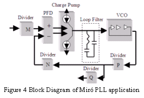
The CP uses a current steering technique and charge sharing when the transistors are switching is reduced thereby reducing the jitter. Statistical variations between nominally matched devices in both the CP and the PFD are taken into account in both the static phase error and jitter constraints. The loop filter is integrated. It is a second order filter used to attenuate control voltage ripple. The voltage controlled oscillator (VCO) is a single-ended current controlled oscillator controlled by a V-I converter. The VCO uses an amplifier in the V-I converter as an 'active-cascode', to improve the power supply rejection ratio. There are also internal decoupling capacitors to maximize the high-frequency power supply rejection.
Miró takes into account a large number power supply noise sources. These include sinusoidal noise sources added at the low frequencies (the crossover frequency), high frequencies, white noise, as well as steps on the power supply. The user can specify the amplitude of each of these different noise sources at the beginning of the optimization process. The user then specifies maximum allowable peak jitter and cycle-to-cycle jitter due to these different sources. In this way the user can ensure the PLL will operate according to specifications in a harsh, mixed-signal environment.
The output of the VCO drives a small-swing to CMOS converter and is then usually divided by 2 to achieve a 50% output duty-cycle. If phase alignment with the on-chip clock is necessary, the user can insert a replica of their clock tree in the feedback path. The divider, if present, will employ a retiming latch to eliminate any jitter added by this block.
The engine takes as user input all of the well known top-level specifications of the PLL. These include specifications on power, jitter, bandwidth, output frequency, PSRR and layout area. Therefore, only an understanding of top-level specifications is required from the user. The process of mapping design specifications to component sizes, transistor widths and lengths and sizes of capacitors and resistors in the PLL is fully automated inside the synthesis platform. The method is process independent, which means that it is easily portable process dimensions shrink, making analog design re-use possible.
4.3 Miró – more detail on GP Implementation
Geometric programming allows design constraints to be formulated hierarchically.
The design constraints of the sub-blocks of the PLL such as the charge-pump and VCO are formulated as a function of their input/output specifications. For example, the output current mismatch of the charge-pump is formulated in posynomial form as a function of the transistor sizes and parameter values of the charge-pump.
Also, important to consider is the threshold voltage mismatch. This mismatch is modeled as the variation between the threshold voltage for a particular transistor and the nominal threshold voltage for the process is modeled as a random variable with the variance inversely proportional to the area of the device. The standard deviation in the current is modeled as the percent variation between the saturation current for a particular transistor and the nominal saturation current for the transistor in the process as a random variable with the variance inversely proportional to the area of the device. Transistors on opposite sides of a differential pair will exhibit mismatch in threshold voltage and saturation current due to random variations that occur during fabrication.
The system level design constraints of the PLL are formulated in terms of the input/output specifications of the sub-blocks. For example, the contribution of the output current mismatch of the charge pump to PLL jitter is written in posynomial form. This hierarchical formulation results in a modular description for the geometric program. It results in better maintainability of the implementation and enables re-use of code when implementing the method for different PLL topologies. For example, if we want to use a different charge-pump in the PLL only the much smaller charge-pump module of the code needs to be updated.
In summary, the design methodology consists of the following steps:
• Defining sub-blocks and corresponding input/output variables. The sub-blocks of a PLL include the phase/frequency detector, charge-pump, loop filter, voltage-controlled oscillator, and divider. Each sub-block has a minimal number of defining input/output variables that are sufficient to describe the behaviour of the PLL and the interaction between sub-blocks. For example, the input/output variables of the PFD include power dissipation, area, reset time, up/down timing mismatch, and output rise/fall time
• Writing (posynomial) equations for input/output variables of sub-blocks in terms of component sizes.
The focus of this paper is not to show the detailed modeling of the components but rather to explain how to expand the methology for higher level blocks.
Writing (posynomial) system level PLL design equations in terms of input/output variables of sub-blocks : at this step, the design constraints of the PLL are put in posynomial inequality form in terms of the input/output variables of the sub-blocks. This step and the previous step introduce a hierarchical methodology for writing PLL design equations in terms of the PLL component sizes. For example, the total power dissipation of the clock generation PLL is given by the sum of the power dissipations of its sub-blocks, i.e.,
The power for each sub-block is one of its I/O variables and can in turn be expressed as a posynomial function of its design variables. Another example is the stability condition for the PLL and this can be obtained by deriving posynomial constraints on the phase margin and gain margin from the loop gain expression of the PLL.
5. Robust IP
The earlier sections described in detail the theory behind the GP implementation to analog IP creation; sections 5 and 6 are focussed on how to use the synthesis platform and IP engine to create optimal PLL’s which are ready for manufacture. Two examples from customer requirements are used.
To carry out a robust optimization of the analog IP ensuring reliability and high manufacturing yield, the IP was optimized over multiple process corners. The term corner refers to the process and temperature variation of the NMOS and PMOS transistor during manufacturing in a semiconductor foundry. Supply voltage variation and on-chip bias resistance variations are included as parameters. In addition to this the user, by means of input parameters, has control over the amount of noise (amplitude, frequency) seen by the PLL on the supply and substrate; the mismatch in transistor threshold voltage and the mismatch in drain current. These are used to calculate several components of the noise in the analog IP.
On a 1.8 V supply, the optimization ensured that all of the specifications were met at both 1.62 V and 1.98 V (Vdd +/- 10%). For example, while power consumption may be worst-case at 1.98 V, saturation margins will be worst-case at 1.62 V. The percent variation of any on-chip resistors: if this value is 20 %, the optimization ensured that all of the specifications were met at resistance +/- 20 %. Since resistors were used in the voltage reference and loop filter circuits, and therefore critical to the manufacturing yield, both reference current variation and stability margins were taken into account during optimization. When the process corners for a robust design are selected, the following occurs:
• Each specification must hold for every process corner and the value of the specification reported is the worst-case value for the set of corners chosen.
• The reported value for the objective is the worst case over the selected corners.
6. Silicon Validation
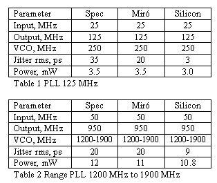
We have used Miró to synthesize a number of PLL’s in 0.25 m, 0.18 m, and 0.13 m processes from both ‘pure play foundries’ and IDM’s. Tables 1 and 2 summarise the key parameters of two PLL’s produced using Miró on TSMC’s 0.18 m logic process. The Miró results are shown for worst case process , voltage and temperature variations. The GDSII layout was produced in a matter of hours and submitted directly to the foundry without any changes.
7. Conclusions
The case for synthesizable analog IP has been proven using geometric programming techniques to produce circuits that are optimally designed to the specification and are robust. This paper described the technique and has verified the design of PLL’s from specification to GDSII on silicon.
References
[1] ‘Electronic design automation’, IEEE Spectrum, B. Martin, 36(1) :57-61, Jan 1999[2] Cahners In Stat. Reports
[3] ‘CAD Tools for Mixed Signal and RFIC’s’ Tutorial, DAC 2001
[4] ‘GPCAD : A tool for CMOS Op-amp synthesis’, M. Hershenshon, S. Boyd, T.H. Lee, IEEE/ACM Conference, San Jose, CA Nov. 1998
[5] ‘Optimization of inductor circuits via Geometric Programming’, M. Hershenson, S. Mohan, S. Boyd, T.H. Lee, 36th IEEE/ACM/DAC Conference 1999
[6] ‘Optimal allocation of local feedback in multistage amplifiers via Geometric Programming’, J.L. Dawson, S. Boyd, M. Hershenson, T.H. Lee, IEEE Transactions on Circuits and Systems I, 48(1) :1-11, January 2001
[7] ‘Geometric Programming – Theory and Applications’, R.J. Duffin, E.L. Peterson, and C. Zener, Wiley 1967
