by Steven Leibson, Tensilica, Inc.
Santa Clara, USA
Abstract:
The emergence of configurable and extensible application-specific processors creates a new SOC design path that is quick and easy enough for the development and refinement of new protocols and standards yet efficient enough in silicon die area and power to permit very high volume deployment.
Reduce SOC simulation and development time by designing with processors, not gates
Rapid evolution of silicon technology is bringing on a new crisis to system-on-chip (SOC) design. To be competitive, new communication, consumer, and computer product designs must exhibit rapid increases in functionality, reliability, and bandwidth and rapid declines in cost and power consumption. All of these improvements dictate increasing use of high-integration silicon, where many of the data-intensive capabilities are presently realized with register-transfer-level (RTL) hardware-design techniques. At the same time, the design productivity gap—the growing cost of nanometer-scale semiconductor manufacturing and the time-to-market pressures of a global electronics market—puts intense pressure on chip and SOC designers to develop increasingly complex hardware in decreasing amounts of time.
One way to speed development of mega-gate SOCs is the use of multiple microprocessor cores to perform much of the processing currently relegated to RTL. Although general-purpose embedded processors can handle many tasks, they often lack the processing bandwidth needed to perform particularly complex processing tasks such as audio and video media processing. Hence the historic rise of RTL use in SOC design. A new class of processor, the extensible microprocessor core such as Tensilica’s Xtensa processor, can be configured to bring the required amount and type of processing bandwidth to bear on many embedded tasks. Because these extended processors employ firmware instead of RTL-defined hardware for their control algorithm, it’s easier and faster to develop and verify processor-based task engines for many embedded SOC tasks than to develop and verify RTL-based hardware to perform the same tasks. A few characteristics of nanometer-scale IC design illustrate the challenge facing SOC design teams:
• In a generic 130 nm standard-cell foundry process, silicon density routinely exceeds 100K usable gates per mm2. Consequently, a low-cost chip (50mm2 of core area) can carry 5M gates of logic today. Simply because it’s possible, a system designer somewhere will find a way to exploit this processing potential in any market.
• In the past, silicon capacity and EDA tools limited the practical size of a block of RTL to smaller than 100K gates. Improved synthesis, place-and-route, and verification tools are raising that ceiling. Blocks of 500K gates are now within the capacity of today’s EDA tools, but existing design and verification methods have not kept and are not keeping pace with silicon fabrication capacity, which can now put millions of gates on an SOC.
• The design complexity of a typical logic block grows much more rapidly than does its gate count. System complexity increases much more rapidly than the number of constituent blocks and verification complexity has grown disproportionately. Teams that have recently developed real-world designs report spending as much as 90% of their development effort on block- and system-level verification.
• The cost of a design bug is quickly going up. Much is made of the rising cost of deep-sub-micron IC masks—the cost of a full mask set is approaching $1M. But mask costs are just the tip of the iceberg. The combination of larger design teams required by complex SOCs, correspondingly higher staff costs, bigger NRE fees, and lost profitability and market share makes show-stopper design bugs intolerable. Design methods that reduce the occurrence of, or permit painless workarounds for such showstoppers pay for themselves rapidly.
• All embedded systems now contain significant amounts of software. Software integration is often the last step in the development process and routinely gets blamed for overall program delays. Earlier and faster hardware/software validation is widely viewed as a critical risk-reducer for new product-development projects.
• Standard communication protocols are rapidly growing in complexity. The need to conserve scarce communications spectrum, plus the inventiveness of modern protocol designers, has resulted in the creation of complex new standards (for example: IPv6 Internet Protocol packet forwarding, G.729 voice coding, JPEG2000 image compression, MPEG4 video, Rjindael AES encryption). These new protocol standards demand much greater computational throughput than their predecessors.
Competitive pressure has pushed us to the next-generation SOC, characterized by dozens of functions working together. Figure 1 illustrates the trend towards the use of large number of RTL-based logic blocks on SOCs and the mixing together of control processors and digital signal processors on the same chip.
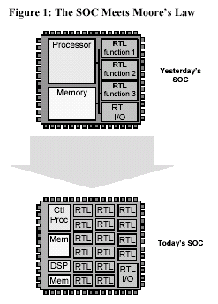
The ceaseless growth in IC complexity is a central dilemma for system-on-chip design. If all these logic functions could be implemented with multiple, heterogeneous processor blocks that were cheap, fast, and efficient, a processor-based design
approach would be ideal because using pre-designed and pre-verified processor cores as individual functional blocks in an SOC moves the SOC design effort largely to software. This SOC design approach permits bug fixes in minutes instead of months because software is much easier to change and verify than hardware. Unfortunately, general-purpose processor cores fall far short of the mark with respect to application throughput, cost, and power efficiency for the most computationally demanding problems. At the same time, custom RTL logic designed for complex functions and emerging standards both takes too long to design and is too rigid to change easily once it’s designed. A closer look at the make up of the typical RTL block in Figure 2, which shows the datapath on the left and the state machine on the right, gives insight into this paradox.
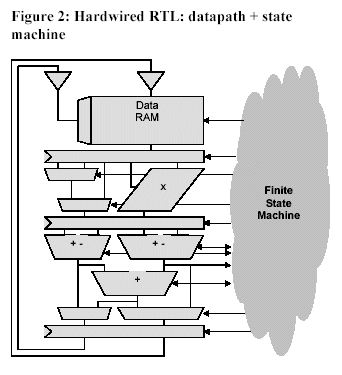
In most RTL designs, the datapath consumes the vast majority of the gates in the logic block. A typical datapath may be as narrow as 16 or 32 bits, or hundreds of bits wide. The datapath will typically contain many data registers, representing intermediate computational states, and will often have significant blocks of RAM or interfaces to RAM that is shared with other RTL blocks. These basic datapath structures reflect the nature of the data and are largely independent of the finer details of the specific algorithm operating on that data.
By contrast, the RTL logic block’s finite state machine contains nothing but control details. All the nuances of the sequencing of data through the datapath, all the exception and error conditions, and all the handshakes with other blocks are captured in this subsystem of the RTL logic block. This state machine may consume only a few percent of the
logic block’s gate count, but it embodies most of the design and verification risk due to its complexity. A late design change made to an RTL block is much more likely to affect the state machine than the structure of the datapath. This situation heightens the design risk. Configurable, extensible processors (a fundamentally new form of microprocessor) provide a way of reducing the risk of state-machine design by replacing hard-to-design, hard-to-verify state-machine logic blocks with pre-designed, pre-verified processor cores and application firmware.
The Promise of Configurable Processors
As discussed above, logic design and verification consume much of the SOC design effort. New chips are characterized by rapidly increasing logic complexity and Moore’s-law scaling makes megagate SOC designs feasible. Fierce product competition in system features and capabilities drives demand for advanced silicon designs. A well recognized “SOC design gap†widens every year. That gap arises between the growth in chip complexity and productivity growth in logic design tools, shown in Figure 3.
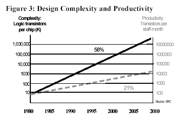
Moreover, the trend towards high-performance, low-power systems (e.g. long-battery-life cell-phones, four-mega-pixel digital cameras, fast and inexpensive color printers, digital HDTVs, and 3D video games) is also increasing the size of SOC designs. Unless something closes this design gap, it will become impossible to bring the enhanced, future versions of these system designs to market.
The Limitations of Traditional ASIC Design
The conventional SOC-design model closely follows the tradition of its predecessor: the board-level combination of a standard microprocessor, standard memory, and logic built as ASICs (shown in Figure 4). Board-level, chip-to-chip interconnect is expensive and slow so shared buses and narrow data paths (often only 32 bits wide) are typical of board-level designs. These relatively narrow buses are often carried over to SOC designs because this design approach, reusing what’s been done before, is the easiest way to architect an SOC.
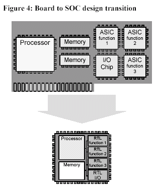
When all of these system components are combined on a single piece of silicon, maximum system clock frequency increases and power dissipation decreases relative to the equivalent board-level system design. System reliability and cost often improve as well. These benefits alone can often justify the investment in an SOC. However, the shift to SOC integration does not automatically change a design’s structure. In fact, the architecture of these SOC chips typically inherits the limitations and design trade-offs of the original board-level designs.
The Impact of SOC Integration
The traditional approach to SOC design is further constrained by the origins and evolution of microprocessors. Many of today’s popular embedded microprocessors (especially the 32-bit architectures of the 1980s such as ARM, MIPS, 68000/ColdFire, PowerPC, and x86) are direct descendants of desktop computer architectures. These processors were originally designed to serve general-purpose applications. Consequently, these processors typically support only the most generic data types (8-, 16-, and 32-bit integers) and operations (integer load, store, add, shift, compare, logical-AND, etc.). The general-purpose nature of these processors makes them well suited to the diverse mix of applications run on computer systems. These processor architectures are equally good at running databases, spreadsheets, PC games, and desktop publishing. However all of these processors suffer from a common problem: their non-specific design dictates an ability to execute an
arbitrary sequence of primitive instructions on an unknown range of data types. Compared to general-purpose computers, embedded systems are more diverse as a group, but are individually more specialized. A digital camera may perform complex image processing but it never executes SQL database queries. A network switch must handle complex communications protocols at optical speeds but doesn’t need to process 3D graphics.
The specialized nature of individual embedded applications creates two issues for general-purpose processors in data-intensive embedded applications. First, there’s a poor match between the critical functions of many embedded applications (e.g. image, audio, and protocol processing) and a processor’s basic integer instruction set and register file. Because of this mismatch, embedded applications require more computation cycles when run on general-purpose processors. Second, more focused embedded devices cannot take full advantage of a general-purpose processor’s broad capabilities so expensive silicon resources built into the processor go to waste because they’re not needed by the specific embedded task that’s assigned to the processor.
Many embedded systems interact closely with the real world or communicate complex data at high rates. These data-intensive tasks could be performed by some hypothetical general-purpose microprocessor running at tremendous speed. For many tasks, however, no such high-clock-rate processor exists today as a practical alternative. The fastest available embedded processors are typically orders of magnitude too costly and dissipate orders of magnitude too much power to meet embedded system design goals. Consequently, designers resort to hardwired RTL circuits to perform data-intensive functions. In the past ten years, wide availability of logic synthesis and ASIC design tools has made RTL design the standard for hardware developers. RTL-based design is reasonably efficient (compared to custom, transistor-level circuit design) and can effectively exploit the intrinsic parallelism of many data-intensive problems. RTL design methods often achieve tens or hundreds of times the performance achieved by a general-purpose processor.
Configurable, Extensible Processors
Like logic-synthesis-based RTL design, extensible-processor technology enables the design of high-speed logic blocks tailored to the assigned task. The key difference is that RTL state machines are realized in hardware and logic blocks based on extensible processors use firmware for this function.
A full-featured configurable processor toolkit consists of a processor core and a design tool environment that permits significant adaptation of that base processor design by allowing a system designer to change major processor functions thus tuning the processor to specific application requirements. Typical forms of configurability include additions, deletions, and modifications to memories, to external bus widths and handshake protocols, and to commonly used processor peripherals. An important superset of configurable processors is the extensible processor—a processor whose functions can be extended by the application developer to include features never considered or imagined by designers of the original processor.
Extensible Processors as RTL Alternatives
Hardwired RTL design has many attractive characteristics—small die area, low power, and high-throughput. However, the liabilities of RTL (difficult design, slow and difficult verification, and poor scalability to complex problems) are starting to dominate. A design methodology that retains most of the efficiency benefits of RTL but with reduced design time and risk has a natural appeal. Application-specific processors as a replacement for complex RTL fit this need.
An application-specific processor can implement datapath operations that closely match those of RTL functions. The equivalent datapaths are implemented using the integer pipeline of the base processor, plus additional execution units, registers and other functions added by the chip architect for a specific application. As an example of how such a processor is defined, the Tensilica Instruction Extension language (TIE is a simplified version of Verilog) is optimized for high-level specification of datapath functions in the form of instruction semantics and encoding. A TIE description is much more concise than RTL because it omits all sequential logic, including state machine descriptions, pipeline registers, and initialization sequences. The new processor instructions and registers described in TIE are available to the firmware programmer via the same compiler and assembler that use the processor’s base instructions and register set. All sequencing of operations within the processor’s datapaths is controlled by firmware, through the processor’s existing instruction fetch, decode, and execution mechanisms. State-machine firmware is written in a high-level language such as C or C++. Extended processors used as RTL replacements routinely use the same datapath structures as traditional RTL blocks: deep pipelines, parallel execution units, problem-specific state registers, and wide data paths to local and global memories. These extended processors can sustain the same high computation throughput and support the same data interfaces as typical RTL designs.
Control of extended processor datapaths is very different from the RTL counterparts however.
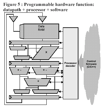
Cycle-by-cycle control of a processor’s datapaths is not fixed in hardwired state transitions but is embodied in firmware executed by the processor (shown in Figure 5). Control-flow decisions occur in branches; memory references are explicit in load and store operations; computations are explicit sequences of general-purpose and application-specific computational operations.
This migration from hardwired state machine to firmware control has many important implications:
1. Flexibility: Chip developers, system builders, and end-users (when appropriate) can change a block’s function just by changing the firmware.
2. Software-based development: Developers use relatively fast and low-cost software tools to implement most chip features.
3. Faster, more complete system modeling: RTL simulation is slow. For a 10-megagate design, even the fastest software-based logic simulator may not exceed a few cycles per second. By contrast, firmware simulations for extended processors run on instruction-set simulators at hundreds of thousands of cycles per second.
4. Unification of control and data: No modern system consists solely of hardwired logic. There’s always a processor running software. Moving RTL-based functions into a processor removes the artificial separation between control and data processing.
5. Time-to-market: Moving critical functions from RTL to application-specific processors simplifies SOC design, accelerates system modeling, and speeds finalization of hardware. Firmware-based state machines easily accommodate changes to standards, because implementation details aren’t “cast in stone.â€
6. Designer Productivity: Most importantly, migration from RTL-based design to application-specific processors boosts the engineering team’s productivity by reducing both the engineering manpower needed for RTL development and verification. A processor-based SOC design approach cuts risks of fatal logic bugs and permits graceful recovery when (not if) a bug is discovered.
Three examples, ranging from simple to complex, serve to illustrate how datapath extensions allow extensible processors to replace RTL hardware in a wide variety of situations. The first example, from the cellular telephone world, involves the GSM audio codec used in cell phones. Profiling the codec code using an unaugmented RISC processor revealed that out of the more than 200 million processor cycles, 80% of the cycles were devoted to executing multiplications. The simple addition of a hardware multiplier would therefore produce a substantial acceleration of this software. Tensilica’s Xtensa processor offers a multiplier as a configuration option. That means that a designer can add a hardware multiplier to the processor’s datapath and multiplication instructions to the processor’s instruction set simply by checking a box on a configuration page of the Xtensa processor generator. The hardware added by checking this configuration box appears in Figure 6.
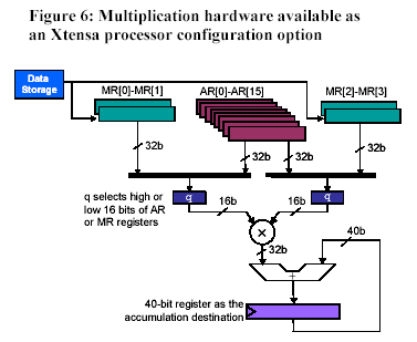
The addition of a hardware multiplier reduces the number of cycles needed to execute the GSM audio codec code from 204 million cycles to 28 million cycles, a 7x improvement in execution time. Adding a few more gates to the processor pipeline by selecting a multiplier/accumulator rather than a multiplier further reduces the number of cycles needed to execute the codec code to 17.9 million cycles. Configuration options coupled with code
profiling allow an SOC designer to rapidly explore a design space and to make informed cost/benefit decisions for various design approaches.
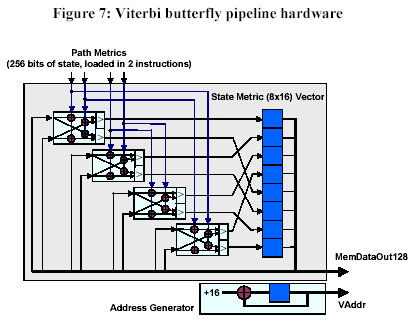
A more complex example, Viterbi decoding, also comes from GSM cellular telephony. GSM employs Viterbi decoding to pull information symbols out of a noisy transmission channel. This decoding scheme employs “butterfly†operations consisting of 8 logical operations (4 additions, 2 comparisons, and 2 selections) and uses 8 butterfly operations to decode each symbol in the received digital information stream. Typically, RISC processors need 50 to 80 instruction cycles to execute one Viterbi butterfly. A high-end VLIW DSP (TI’s 320C64xx) requires only 1.75 cycles per Viterbi butterfly. Tensilica’s TIE language allows a designer to add a Viterbi butterfly instruction to the Xtensa processor’s ISA, the corresponding pipeline hardware shown in Figure 7, and the processor’s configurable 128-bit I/O bus to load data for 8 symbols at a time. These additions result in an average butterfly execution time of 0.16 cycles per butterfly. An unaugmented Xtensa RISC processor executes Viterbi butterflies in 42 cycles, so the butterfly hardware (approximately 11,000 additional gates) achieves a 250x speed improvement over the base-case RISC processor.
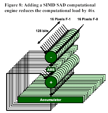
The third example, MPEG4, is from the video world. One of the most difficult parts of encoding MPEG4 video data is motion estimation, which requires the ability to search adjacent video frames for similar pixel blocks. The search algorithm employs a SAD (sum of absolute differences) operation involves a subtraction, taking the absolute value of the subtraction, and then accumulating that result across the entire video frame. For a QCIF (quarter common image format) video frame at 15 frames/sec., the SAD operation for motion estimation requires just over 641million operations/sec. As shown in Figure 8, it’s possible to add SIMD (single instruction, multiple data) SAD hardware capable of executing 16 pixel-wide SAD instructions per cycle using TIE. (Note: Using the Xtensa processor’s 128-bit maximum bus width, it’s also possible to load 16 pixels worth of data in one instruction.) The combination of all three SAD component operations into one instruction and the SIMD extension of this instruction that computes the values for 16 pixels in one clock cycle funnels the 641 million operations/sec. requirement into 14 million instructions/sec., a reduction of 46x.
Conclusion
The migration of functions from software to hard-wired logic over time is a well-known phenomenon. During early design exploration of pre-release protocol standards, processor-based implementations are common even for simple standards that clearly allow efficient logic only implementations. Some common protocol standards that have followed this path include popular video codecs such as MPEG2, 3G wireless protocols such as W-CDMA, and encryption and security algorithms such as SSL and triple-DES. The speed of this migration, however, has been limited by the large gap in performance and design ease between software-based and RTL-based development. The emergence of extensible, application-specific, embedded processors creates a new SOC design path that is quick and easy enough for the development and refinement of new protocols and standards yet efficient enough in die area and power to permit very high volume SOC deployment.
