By Andy Grouwstra, Perceptia Devices
Digital PLLs outperform analog PLLs in jitter, phase noise, power, and die area. They also reduce migration risk and cost. They make integration and production test easy. Yet, they have not been widely available. This will change. Perceptia's newly introduced pPLL08 second-generation digital PLL IP shows that the highest performance requirements can be met. A first version of the IP is optimized for 5G base station operation. It can be paired with the highest performing ADCs and DACs. Yet, its size and power are modest. The IP is expected to change the way that radio designers approach their project.
This article compares analog, first-generation digital, and second-generation digital PLLs. It evaluates which type of PLL may be best in which situation. It further discloses a roadmap into other application areas, including general purpose / logic clocking, and regular low-jitter PLLs.
Some History
The phase-locked loop (PLL) was invented at least as far back as 1932, when a Frenchman, Henri de Bellescize, published a series of four articles in L'Onde Electrique (The Electric Wave) about synchronous reception. He proposed a circuit with just two triodes that locked the frequency of an oscillator one-on-one with the frequency of a reference signal. Today, we would find it mind-boggling that he made a PLL with the equivalent of just two transistors. Monsieur de Bellescize would have found it mind-boggling that in 2019 we use the equivalent of 100,000 or more triodes. Of course, in his time that would have taken quite a building, not to mention a megawatt of power.
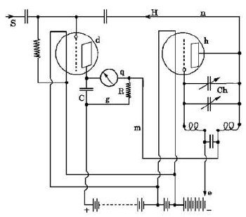
His PLL was analog. It seems that since the early 1960's engineers and researchers have also been discussing digital PLLs. But here we are in 2019, and most PLLs in use are analog. However, there's been some progress. In the late 1990s, Texas Instruments started selling chips for parts of digital PLLs. And, in pockets of Europe, companies have now been using completely integrated digital PLLs for a couple of years. Perceptia Devices, Inc. has offered first-generation digital PLLs ("all-digital PLLs") for ten years.
Most PLL IP companies only offer analog PLLs. It isn't strange that the misunderstanding exists that, for some reason, digital PLLs might not be every bit as good as analog PLLs, let alone be better.
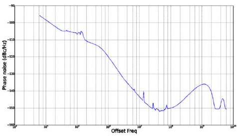
Perceptia has focused on creating various custom and/or high-end versions. Its family of first-generation PLLs is publicly available in only a few dedicated process nodes. The custom projects have illuminated the areas where improvements were possible, some of which are applicable to both analog and digital PLLs, and others only to digital PLLs. Perceptia started pioneering, and has come up with a slew of innovations to improve the jitter, power, and die area. It has a rapidly expanding portfolio of patents and patent applications that protect, and document, its technology. It has combined many of those innovations in a second-generation digital PLL, called pPLL08. pPLL08 has its initial implementation in UMC 40LP. It beats any spec previously seen in the market, with 300 fs RMS, integrated from 6kHz to 700MHz. In our view, these results would not have been possible with an analog PLL.
Let's look at the differences between analog, first-generation, and second-generation PLLs. Then let's look at which PLL is best in which situation, and then let's look a bit deeper into pPLL08 and second-generation PLLs.
Analog PLL
An analog PLL usually contains a voltagecontrolled oscillator (VCO) that delivers the output signal. Feedback and reference blocks contain programmable dividers that feed into a phase-frequency detector (PFD) that compares the feedback clock with the internal reference clock, producing pulsewidth modulated positive or negative pulses that are proportional to any measured differences in phase. A charge pump amplifies these pulses and feeds them to the loop filter, an analog filter that outputs the control voltage for the VCO.
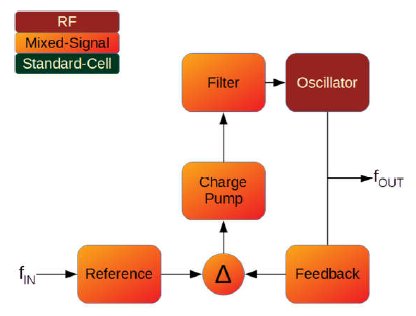
The oscillator is an RF/mixed-signal block, whose performance is critical for the performance and final characteristics of the PLL. The filter is a bulky standard analog block. All other blocks are mixed-signal (discrete level, continuous time). Their design and sensitivity to corner conditions directly impact noise levels and accuracy of the PLL. Their layout is critical. Signal integrity is critical. Designs are impacted by device inaccuracy, and sensitive to noise and interference. Analog PLLs poorly take advantage of process scaling. For example, when migrating an analog PLL from 55 to 28nm (a 49% reduction of line widths), its area might be reduced with only 30% or less.
First-Generation Digital PLL
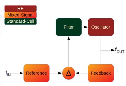
A first-generation digital PLL follows the architecture of an analog PLL. However, the filter is digital, and the oscillator may be digitally-controlled (so it is a DCO rather than a VCO). The filter can directly take an output signal from the PFD, so no charge pump is needed. The filter can be implemented with standard cells, and may be synchronously clocked by the reference frequency fIN. The feedback and reference blocks, as well as the PFD, may be identical to the ones seen in an analog PLL. Therefore, those blocks have the same disadvantages. Nevertheless, the architecture has several advantages, including that the filter scales much better with the technology. It is programmable and flexible. When migrating from 55 to 28nm, a PLL's area might be reduced by about 50%.
Second-Generation Digital PLL
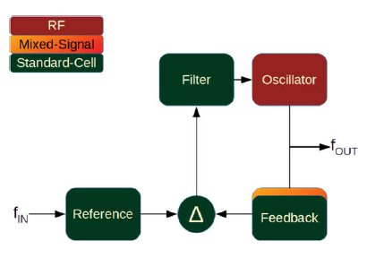
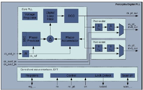
In a second-generation digital PLL, just about everything other than the oscillator is digital and synchronous, and can be implemented with standard cells. The feedback circuit no longer contains a programmable divider. High-performance designs may still include a small mixedsignal block (a TDC, or time-to-digital converter). But in logic clocking PLLs, or regular low-jitter PLLs, this is not necessary. No switched capacitors are needed, or any other mixed-signal technology. The feedback block may contain a phase accumulator, a circuit that measures the phase of the oscillator output signal. The reference block may contain a phase predictor, a circuit that calculates the desired phase based on the user-programmed PLL multiplication factor, which may be integer-N or fractional-N. The phase comparator becomes a simple digital subtractor, subtracting one number from another number. About 99% of the PLL's transistors are part of the RTL-based logic.
Apart from scaling (an area reduction approaching 75% going from 55 to 28nm), second-generation digital PLLs offer many advantages. Clearly, the cost and technical risk of porting between process nodes is much reduced. But also, a PLL's behavior and performance is much better predictable, since the digital parts can be modeled very exactly, whereas the oscillator can be reasonably predicted by extrapolation or interpolating earlier achieved results in similar or adjacent process nodes. For the user, it is much easier to integrate the block, since a much smaller part of the circuitry is analog and sensitive to interference. Testing is also much easier, since the RTL-based logic has scan chains.
Doesn't A DCO Have Quantization Issues?
This is a reasonable question to ask, right? Well, of course it does have quantization noise, just like an ADC or DAC. But, if you remember that the most delicate audio is sublimely rendered by a 1-bit DAC, so can the quantization noise of a DCO be overcome by moving quantization energy from frequencies where it hurts to frequencies where it is harmless. As a result, the current pPLL08 implementation has one of the lowest ever noise profiles, combined with a fractional frequency resolution of 24 bits. This means that even with a 100MHz reference clock you will have an output resolution of better than 6Hz. Quantization? No problem!
When Would You Use a PLL Like This?
There are a few situations where it makes sense to keep using an analog PLL. For example, the PLL you need is already proven in the process you want and in your application; you don't need to worry about die area; and you can live with the limitations of a rigid one-size-fits-all loop filter. But if the PLL you need is not proven in the foundry node you need, or it is an advanced foundry node with high MPW cost, or the process is so new that it is still being tweaked and its models are changing, or the PLL area is critical, or the performance is critical over all process corners, or its behavior must be accurately predicted, or you have a very low supply voltage, or you need very high testability, for example for an automotive application, or your filter must be flexible or optimized for your application, or you need a fast lock, or you need to hold the frequency when your reference drops away or is untrusted, then you should seriously think about a digital PLL. But you should also look at the process node.
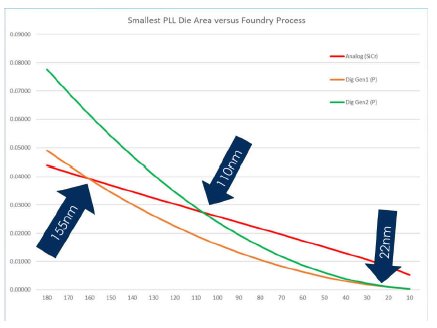
For example, if the size of a PLL is critical for you, then an ultra-high-performance digital PLL will only be a little bit smaller than an analog PLL, no matter how advanced the process is. For a general purpose PLL, a logic clocking PLL, or a lowjitter PLL (all of which can use ring oscillators), the difference can be huge though. The above graph shows that firstgeneration PLLs are smaller than analog PLLs once you go below 155nm. At 22nm, a digital PLL is roughly 10 times smaller. Second-generation digital PLLs are smaller than analog PLLs once you go below, roughly, 70-110nm, and smaller than first-generation digital PLLs once you go below 22nm.
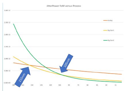
If jitter and power are equally critical to you, then second-generation digital PLLs are best below roughly 105nm. However, first-generation digital PLLs can be pretty good, too. They just don't have the same migration advantages that a second-generation digital PLL offers. If jitter (or phase noise) is more important to you even than power, then second-generation is clearly preferable. It can reach a higher performance, and with better predictability.
pPLL08 Is in Mass Production Now
Based on preliminary characterization results, Perceptia's lead customer for pPLL08 has now taken it in mass production. The initial version, which is offered as pPLL08-5G-U40LP-8G is optimized for a 5G application (perhaps a base station) and features 300 femtoseconds of RMS jitter, integrated over a band from 6 kHz to 700 MHz. Generally, less jitter means more power, but even so, pPLL08 uses only 70mA. Most applications won't need such a high performance, and in other process nodes we may optimize differently. For example, a SerDes may need extremely low jitter too, but integrated over a much smaller band. Or, a PLL in a 5G handset may need to be manufactured in a 7 or 10 nm process, and accept more jitter, but it will have very tight specs on power dissipation. The same goes, in a somewhat larger process node, for Bluetooth LE or narrowband IoT.
Roadmap
Perceptia is member of two foundry IP alliances: GLOBALFOUNDRIES (FDXcelerator™) and UMC. It plans to not only have pPLL08 in selected advanced processes, but also a logic clocking or general-purpose PLL (pPLL02 and lowvoltage version pPLL02LV), a low-jitter PLL (pPLL03), and later a ULP PLL (pPLL09). Migrations of pPLL08 will be targeted at digital radio and/or SerDes, and may be optimized for 5G, Bluetooth LE, NB-IoT, etc. Perceptia further plans a jitter attenuator (pPLL88) based on pPLL08, in a customer-selected process.
The Author
This article was written by Andy Grouwstra, CEO of Perceptia Devices, Inc. Contact information is available on Perceptia's website www.perceptia.com.
