by Tim Daniels, LSI Logic
Bracknell, UK
Abstract:
The first quarter of 2003 will herald the first 90nm prototype capability. However, much of the industry views the latest node with some trepidation given the physical technology challenges that emerged in the move to 0.13ìm.
This paper outlines the various issues found at the latest 0.13ìm node and how these are being solved by the industry and adopted for 90nm design so that time to market compared to previous generations does not become a crippling issue. It is a general paper intended to update those involved in SoC and IP design on current implementation challenges.
Topics discussed include: Voltage, power and reliability issues at the micro level and RTL Analysis, Hierarchical design and database needs at the macro level. Example methodologies used to overcome these issues are given in order to demonstrate solutions for 90nm design.
1.0 Introduction
To design a System-On-Chip (SoC) in 90nm Technology designers simultaneously juggle the dual challenges of controlling both the macro level with big complexity issues and the micro level with small physical issues whilst keeping to the overall constraint of Time-to-Market (TTM) in order to get a return on investment.
The complexity at 90nm is daunting. A 10x10mm die will be able to contain huge SoC functionality. An example of a typical 100mm2 design could be:
| Logic | 10M Gates (20 x 0.5Mbit blocks, inc CoreWare) |
| Memory | 39Mbits (200 instances: 1,2,4 Port Sync) |
| Package | Flip-Chip 960 (with matched pairs) |
| Clocks | 25 (%/MHz: 50/100, 25/200, 25/400) |
| CoreWare 4 off | MIPS5Kf + peripherals, ARM7 + peripherals, 2x40Gbit SFI5/SONET I/F, 10Gbit Ethernet/XAUI I/F, |
Table 1: Example possible 90nm SoC complexity
2 Micro Level Issue
Physical issues that designers face increase dramatically below 0.18um. At 90nm the SoC designer is faced with an array of issues. Key amongst these are: power drop, instantaneous voltage drop (IVD), clock, Crosstalk, and reliability issues (electromigration, yield enhancement). All such design integrity issues must be solved for timing, area and power simultaneously to get a working overall solution.
2.1 Changing Nature of Delay
Over recent technologies the nature of delay has changed from being within the cells to being within the interconnect technology.
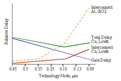
Fig 1: Relative cell to interconnect delay
Switching from Aluminium/SiO2 to Copper/Lowk has helped reduce this effect but in 90nm interconnect delay will dominate with approximately 75% of the overall delay [Ref 1]. Thinner tightly packed interconnect are the root cause for many of the micro level issues discussed below.
2.2 Power Drop
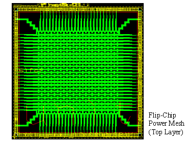
Fig 2: A Flip-Chip power mesh
Ensuring an adequate power mesh is one of the biggest issues. At 90nm only 1v is available in the core so for less than a 5% voltage drop only 50mv drop is allowed across the mesh. The mesh construction is highly dependent upon the number of metal layers, sub-module and memory placement and package type. LSI Logic uses in-house tools to automatically generate a correct by construction power mesh.
Instance based power estimation techniques are used to analyse IR drop to ensure requirements are met. With such little headroom for voltage variation implementation of power mesh will be key.
2.3 Instantaneous Voltage Drop
Peak dynamic power usage, already important at 130nm, will be essential at 90nm. Instantaneous voltage drop (IVD) issues will require close analysis and the insertion of local on-chip capacitors to avoid issues resulting from excessive noise on the power mesh. Areas of high power usage within the die, especially memory, PLLs and clock drivers, will have to be handled very carefully in this respect. LSI Logic uses in-house tools to pre-place on-chip capacitors close to these blocks to avoid IVD failures. In addition on-chip capacitor are also added post-placement in order to reduce effects of IVD on the die. The amount of capacitance added depends on the switching activity (frequency) of the die and the types of cells used.
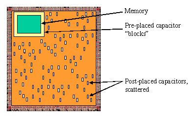
Fig 3: Concept of the IVD avoidance
Another method of reducing IVD now used is by replacing standard flip-flops with slower switching versions during the physical optimisation step of timing closure where the paths have sufficient slack time to stand this. Special Flip-flops are designed for the library specifically for this purpose.
2.4 Clock
At 90nm clock delay and skew will be very difficult to control. The best flows will be based around automated useful skew techniques and will control delay through branches of the clock by adjusting delay via post-clock insertion delay cell swapping. LSI Logic uses “lsimrsâ€, its physical optimisation tool, to insert clock trees with useful clock skew. Clock crosstalk avoidance (via signal wire isolation) is built into such tools in order that the clocks are not aggressors or victims to nearby signal nets.
A side benefit of useful clock skew will be to somewhat reduce IVD issues on the die by spreading the clock edges along different clock branches.
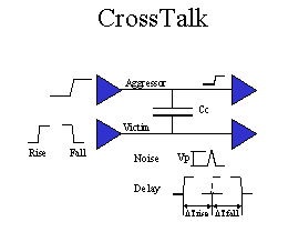
Fig 4: Graphical description of Crosstalk
2.5 Crosstalk
Crosstalk already a common signal integrity issue at 180/130nm, yet often ignored in many SOC flows today, will become critical at 90nm. Crosstalk is caused when an aggressor net running parallel to another victim net causes false switching (noise) or altered timing (delay) on the victim net. Careful analysis, particularly of the delta timing caused by the delay effects, takes roughly two weeks for a 3M gate design. This directly affects layout turn-around-time.
An alternative flow that LSI Logic uses is to add crosstalk avoidance placement/optimisation tools to add margin to the wire delays calculated in the layout tools and SDF timing file (lsidelay tool) in order avoid having to run these crosstalk avoidance analysis tools at all. This does not work for all designs since those pushing timing cannot stand the extra margin. In this case these extra margins have to be overridden and the extra crosstalk analysis tools are run instead.
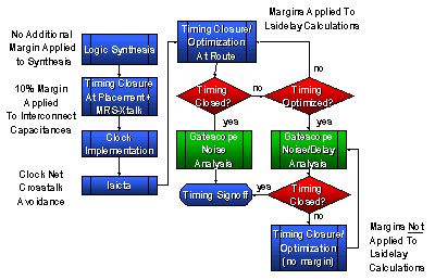
Fig 5: Crosstalk Avoidance Flow
Automated avoidance during routing will eliminate such issues when these tools truly come on-line but such tools are not available today.
2.6 Reliability Issues
Many of the reliability issues seen at 130nm are already addressed via tool automation and methodology changes. These include:
• Metal antennae effects - where an electron charge can build up on long nets during manufacturing and blows up the transistor connected to it. Avoided by inserting diodes or adding metal jogs to the routing to force a layer change. The latter can cause many extra vias in the layout which has it’s own reliability issues if not carefully controlled.
• Metal Slotting effects – this is where wide wires cause “metal dishing†effects due to processing limitations. Avoided by splitting wide wires.
• Simultaneously Switching Outputs (SSO) – where noise is injected into the power rails from many output changes at the same time and causes false signal values. Avoided by adding power/ground pads and by I/O isolation.
• Soft Errors – Alpha particles, both naturally occurring and from lead in packaging, can cause state inversion of a flip-flop or memory element. With shrinking technology the charge induced becomes more significant. Avoided by hardened flip-flops, error correction built into the memories and by fault tolerant system architectures.
• Memory yield – With memory taking an ever-larger proportion of the die, roughly 60% in the example above, overall good die per wafer will be lower than with pure logic. Avoided by adding redundant rows/columns and using Built-In Self Repair (BISR) with the larger embedded memories.
2.6.1 Electromigration
Electromigration (EM) is a key reliability effect that will worsen in 90nm. EM is caused by decreasing metal widths and increasing current density. When overstressed metal ions tend to migrate over time eventually causing the connection to break. LSI Logic runs “lsisignalem†after placement to set routing rules to ensure that metal and via structures are robust enough to avoid the EM issues that can occur on signal nets. Post route checking is also performed to ensure that the avoidance was successful.
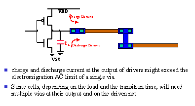
Fig 6: Electromigration avoidance
2.7 Timing Files
One of the “small†issues that are not under control in all flows today is that of accurate delay calculation. Metal variation at 90nm will cause a vast difference in both resistance along the wire and capacitance between the wires. The overall max/min delay numbers are a complex equation of rise time along the nodes varying with R and C, where the worst case R and C does not necessarily give the worst case delay numbers. LSI Logic uses “lsidelay†to generate accurate golden timing information from the RC data, which may be run on multi-processor machines for speed. Generating real best and worst case numbers from extracted R/C data is a non-trivial task where over-simplified algorithms will start to fall apart in 90nm. The tool can also handle varying PVT (Process/ Voltage/ Temperature) and other factors that affect the overall timing.
2.8 Metal Stack
Another more physical issue, not under control in all processes today, is that of the manufacturability and reliability of the copper/Low-K metal stack [Ref 2]. At 0.18um LSI Logic qualified Low-K with an aluminium metal stack. The low-K dielectrics gave huge benefits in terms of reducing the effects of coupling capacitance of the interconnect. At 0.13um LSI Logic used both Low-K and a copper metal stack. Switching from aluminium to copper has been a steep learning curve for the industry but having got this under control moving to the 90nm technology node will be relatively straightforward since the same basic materials will be used in the metal stack.
3 Macro Level Issues
When dealing with the “big†complexity issues, SoC design teams are being forced to face new challenges of defining and fixing system architectures based around truly market-available IP and then integrating in-house designed blocks as needed to complete the functionality. Controlling the “big†boils down to: picking the right IP to suit the architecture (and vice versa), developing a solid software and early hardware verification strategy, performing early RTL analysis on developed code, early physical planning, a complete test strategy all coupled closely with tough project management and business skills.
3.1 Physical RTL optimisation
Physical RTL optimisation analysis is now being recognized by the industry as an important tool for SoC designers, with a variety of EDA tools becoming available. Such tools comprehend the physical implementation of the RTL and give early feedback as to poor RTL constructs that will cause problems in layout.
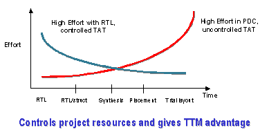
Fig 7: Early RTL analysis gives project control
Good RTL architecture and coding can save many man months in project timescales. The RTL analysis tools within LSI Logic’s FlexStreamTM design flow perform fast synthesis, partitioning, placement, and timing analysis of an RTL block and provide detailed information about that block.
Such a tool highlights issues in the RTL that are likely to cause problems for the layout tools later in the flow. LSI Logic rules built into the tool specifically highlight RTL constructs that have caused problems in the past. Designers armed with this knowledge can then modify the architecture and coding of the RTL to avoid such issues.
One example of typical issues is RTL that infers a huge mux’ing function, common in communication switch SOC’s, which will be difficult to layout. One alternative would be to split the mux’ing function in a different way. A second example is that of a controller block that is shared between two sub-modules and is in the critical timing path for both modules. One solution to this is to duplicate the controller function locally to each.
The best RTL Analysis tools therefore provide an idea of the physical issues that have been inferred in RTL code even before floorplanning is started. They provide very fast feedback on how to optimise the architecture and coding which is linked directly back to the source RTL code, in a way that early floorplanning/placement tools simply cannot.
3.2 Floorplanning
Early physical planning of big SoC designs is a pre-requisite. An early floorplan showing location of the high speed I/O, block and memory location quickly gives an idea of the feasibility of the physical design and goes one stage further than the RTL Analysis tools. For example, the SFI5 physical layer interface in the design example is complex - 16 differential pairs making 40Gbit/s (16X2.5Gbit/s) - and requires careful placement on the die, the package and the board. Such system level skill sets are non-trivial and highly sought after in order to drive products quickly to market with low risk. Floorplanning a 10Mgate design requires detailed routing of global signal and clock nets at this early stage in order to control time of flight and define timing and area budgets for the block. Modern tool flows, such as the FlexStream Design System, allow hierarchical design approaches for each of these sub-blocks but it is controlling timing closure early at this top level that is the key to a fast turn-around-time and eventually a successful product.
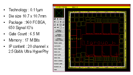
Fig 8: Typical Floorplan at 0.13um
4 Cross-Border Issues
There is a further category of issues that crosses macro and micro levels, including test, overall chip power/temperature and database size, that will challenge engineers in 90nm. Among the test issues: Traditional “full scan†stuck-at fault coverage test strategies are starting to take too long in production testing and are increasingly shown to have too many test escapes, IDDq testing is becoming less viable due to increasing transistor leakage. Silicon vendors, EDA companies and research institutes are actively working on such issues and we are likely to see fast evolving test strategies in the near future including Scan compression, Logic BIST, and transition fault coverage.
Overall chip power will become an increasing focus for SoC in 90nm because die temperature has a direct effect on failure rate and therefore the reliability of the SoC. Approaches used in battery-operated devices for years, such as slow clocking and sleep modes as well as the more usual gated clocking, grey code addressing and memory splitting will be widely used. EDA tools will have to truly consider the third axis of power (as well as time and area) within the design flow.
4.1 Database Sizes
The last cross-border challenge to be highlighted is that of file and database size. An example of controlling database size, and therefore turn-around-time, is that of the typical timing signoff flow today: SPEF files (RC data) are extracted at chip level, then SDF files are generated using the silicon vendor’s golden timing engine and an STA tool will analyze this database. Final flat timing runs like this already take several days, each intermediate file taking several Gbytes of data, and running only on a machine with a 64bit operating system. Short term, key tools such as LSI Logic’s delay calculator “lsidelay†that generates the SDF have been adapted to run on multi-threaded and multi-processor compute farms. Longer term the industry will adopt methodologies such as OLA library models (a library with a built in golden timing calculator supplied by the silicon vendor) and OpenAccess common databases such that extraction, delay calculation and STA analysis can be accomplished in a much more efficient manner. Using a single database into which all tools can plug will completely avoid the many intermediate files of varying formats with differing limitations being required. [Ref 1].
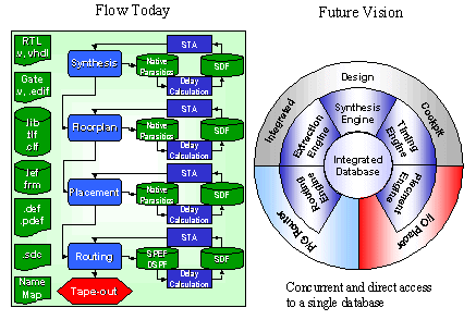
Fig 9: File and database issues
In general, the management task of generating and controlling a machine, software and human resource infrastructure to enable SoC design within time-to-market constraints could end up being the biggest challenge of all. This is especially true as it involves the cross-industry collaboration of silicon vendors, EDA vendors and system houses.
5 Summary
When looking at volume production requirements the need for lowest cost, smallest die, lowest power and fastest speed will always push SoC design teams to the leading edge of technology. Foundries are already running early 90nm silicon at an R&D level and early SPICE rules are already available. First sign-off cell libraries are now available while the first IP blocks will be available during the first half of 2003 along with prototype capability.
Whilst some may believe the industry is at its lowest ebb for years with balance sheets showing red in many industry sectors, there is already a 90nm SoC infrastructure being put in place that will yield leading edge products within the next year. For SoC designers, the need to grapple with the technology challenges of 90nm will be here sooner than many had dared hope.
References:
1 Down to the Wire, Lavi Lev et al, Cadence
http://www.cadence.com/feature/pdf/4064_NanometerWP_fnlv2.pdf
2: Failures plague 130-nanometer IC processes, Ron Wilson, EETimes
http://www.eetimes.com/story/OEG20020826S0022
