By Amol Agarwal, Vandana Sapra (NXP India)
ABSTRACT
The design complexity of sub-micron designs due to ever growing huge number of gates and interactions has made it difficult for physical design tools to handle the physical synthesis or placement and routing of such SOCs. Hence design partitioning plays a critical role for implementation of such design which deploys divide-and-conquer strategy.
Conventionally, RTL designer tries to split the complete design in different partitions keeping functional perspective but many a times such design are not backend friendly. RTL designer relies on backend feedback which becomes an iterative process with huge turn around time. Through this paper, we are proposing a technique which focusses on smart port reduction methodology which would list all the possibilities of efficient partitioning with reduced ports count of each partition.
1. Introduction
The advancement in semiconductor technology has made possible high number of cells to be intergrated on to a single chip. The cell density has increased to a level that it cannot be efficiently handled by all physical design tools without posing various challenges in routability and timing closure, hence design partitioning has become an important aspect of SOC design.
Design Partitioning means dividing or decomposing the complete design in separate components which can be then individually synthesized, closed and then integrated in complete design speeding up the design process.
Logical or physical partitioning challenges are not new for chips targeted for wireless and networking applications. Over the years, EDA tools has adapted to partitioning challenges associated with these type of designs. There have been various automations and algorithms designed for same but for automotive chips this is relatively difficult problem statement which has not been completely addressed.
Due to emerging safety trends in automotive sector, the design implementation has increased in complexity because of certain unique requirements like true online logic built-in self-test (LBIST), in which a part of a design is expected to be completely functional while there is self-test running on rest. Moreover, the test coverage requirement for such integrated-chips has also become stringent because of which there is lot of on-chip DFT logic. Typically, area overhead associated with DFT and self test logic is somewhere in range of 25-30% of standard cells area. As a result , it is quite challenging for such chips to define clean physical partitions having standard interfaces.
2. Design Challenge
Conventionally, RTL designer tries to split the complete design in different partitions with various goals in mind.
First, of achieving manageable gate count in each partition.
Secondly, each partition in sync with safety requirements to meet LBIST requirements.
Third, the port count of each partition is minimum as possible as it causes routing congestion and timing issues around interfaces. The blocks interacting more functionally are kept in same partition so that there is minimum interaction between partitions.
Inefficient partitioning may lead to smaller partition sizes but with very huge pin count. This could turn out to be very serious problem because it is difficult to place so many ports over smaller edges. As a result floorplan designer is forced to place ports close to corners of hard partition since space in middle of partition edge is not sufficient to place all the ports. However, placing too many ports close to corner of partition may lead to huge routing congestion issues which is not a easy problem to solve.
As shown in Figure 1.0 below (taken from real SoC), design has no routing congestion elsewhere except at partition corners. This is because too many ports are placed near to partition corners and P&R tool does not have enough routing resources to route nets connected to partition ports and top level nets turning around partition corners.
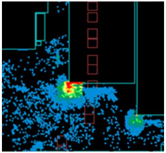
Figure 1: Routing congestion around corners (SOC snapshot)
Hence it a challenge to create partitions of optimum size with minimum port count.
All the approaches to target third goal is iterative. RTL integration designer tries to minimize the ports of a physical partition by assuming all the blocks interacting if kept in same partition would lead to optimum port count, but there is no tool or methodology to verify this assumption and to find out if there are more such opportunities in design to reduce port count.
Unlike chips having no LBIST requirements, it is not prudent to define physical partitions on the fly in P&R tools because you cannot split LBIST logic across physical partitions.
3. Methodology
This paper describes a smart port reduction methodology which would list many such possibilities of reducing port count of a partition which generally gets ignored during design stage. There have been cases observed where RTL designer sometimes misplace some instances on top or in other partition leading to redundant port creation at partition level. This methodology looks for three different kind of opportunities explained in detail below. Its results are potential candidate of hierarchy movement in design or pin placement movement in floorplan which can be evaluated by RTL and backend designer.
3.1 Loop-back irregularity
If single or multiple ports of a partition, enter a single input or multiple input combinatorial logic respectively present outside of partition and its output re-enter the partition. There is high probability that combinatorial logic placed outside of a partition can be moved inside a block as inputs emanate from the partition and terminates inside the partition as shown in Figure 2.0
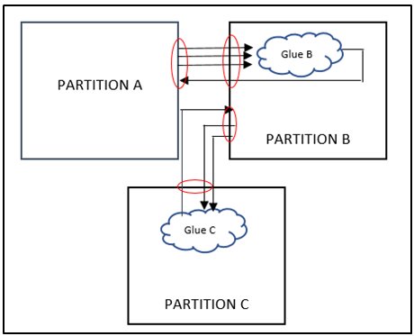
Figure 2: Loopback irregularity
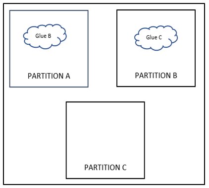
Figure 3: Loopback irregularity (fixed)
In example shown above, Glue B present in partition B has inputs coming from partition A and output going back to Partition A creating 4 extra ports at partition A as well as Partition B. This could be case if say memories of a block are placed in Partition A but related glue logic Glue B around the memory controls gets mistakenly placed in Partition B. Now if Glue B is placed in Partition A , it leads to overall port reduction of 8. Similarly if , hierarchy of Glue C is changed to Partition B, overall 6 ports can be reduced as shown in Figure 3.0.
There can be many efficient ways to report such cases in design. One such way is described below.
- Report all such output ports of partition A as start point which have endpoints in partition A itself.
- For all such output ports, report fanout.
- For all combinational cells reported in fanout, check if other inputs are only coming from partition A , then that combinational logic can be moved in partition A.
3.2 Quiescent congestors
In this technique we try to find out passive congestors as indicated by the term “quiescent” which means “in a state or period of inactivity”. Many a times there are ports on hard partition which have no good role to play and are redundant. This may happen because of various reasons ex: Integration tool creates extra ports on the hard partition while creating port of bus type or a highly resuable multifunctional IP with lot of miscenallenous interfaces is being integrated with all of its ports present on hard partition, out of which only few are going to be functionally used.
To find out such instances,
- Check for the connectivity of all the input and output ports of a hard partition.
- Input ports which are tied to a value and Output ports which are not driving any logic at all are proposed to be removed and if cannot be removed due to reusability issues are suggested to be placed on extreme sides of a partition so that they do not interfere in routing and placement of other ports. This needs to be approved by RTL designer to make sure there is no planned change for the connectivity of those ports.
The other category is cases in which an output coming out a hierarchy present in partition has all its inputs also coming from different partitions which indicates that block has no role in that partition and only creating extra ports and area to that partition as shown in Figure 4.0.
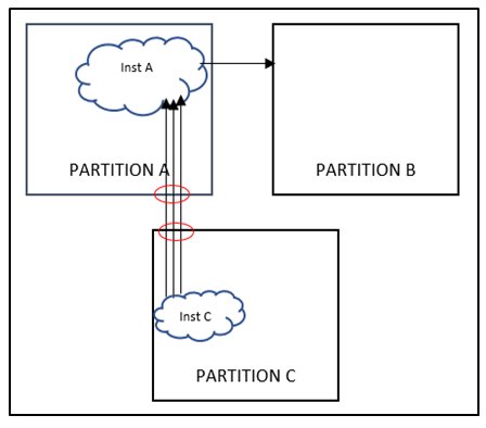
Figure 4 Quiescent Congestion
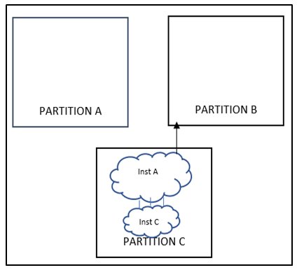
Figure 5: Quiescent Congestion (fixed)
To find out instances violating in second category mentioned above,
- Connectivity of all ports of submodules inside a hierarchy is dumped.
- If both input source and output destination are reported to be present out of current partition. That submodule is real candidate of movement outside of that partition.
- If total number of ports of this sub-module is p and for greater than p/2 ports, source or destination is outside of partition, even then that sub-module is potential candidate for movement and will help in reducing count of ports on partition.
3.3 Extramural re-convergence/divergence
Extramural means “outside the walls”, hence this technique reports cases where reconvergence/divergence is happening outside the walls of hard partition. In first caregory, It lists out the cases where multiple ports say N ports of a partition are reconverging in a multi input combinatorial gate or logic present outside of partition, its output may be consumed of outside of partition but by pulling in this hierarchy will result in reduction of N-1 ports.
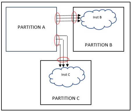
Figure 6: Extramural reconvergence
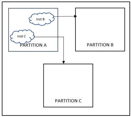
Figure 7: Extramural reconvergence (fixed)
As shown in figure 6.0, Inst B and Int C present inside Partition B and Partition C respectively have inputs coming from Partition A, the output of these instances is consumed inside partition B and Partition C only but if these instances are moved inside Partition A , it would lead to multiple port reduction. For example, if there are certain faults or debug related signals getting captured in fault monitor unit or debug mux respectively present in Partition B where all faults are getting ored/muxed in Inst B. So if the OR/MUX gate gets moved inside Partition B, there will be significant port reduction on Partition A as well as Partition B.
To find such opportunities,
- Report all fanout of all output ports of partition A.
- Save all the fanout of all the ports in an array.
- For the instances, where the number of occurance is more than one, shows there is reconvergance.
- Such instances can be moved to Partition A.
To understand the above algorithm, let’s take an example. For simplification purpose, limited number of ports and partition are considered.
Say, fanout of ports A1 is B/U1 and B/U2 where B indicates the B partiion and U1 and U2 are combinational gates. So we have an array like [ {A1, B/U1} , { A1, B/U2}]. Similarly fanout of port A2 is B/U2. Fanout of A3 is B/U1 and so on.. If content of all such arrays are appended, we will get a new array like [ {A1, B/U1} , {A1, B/U2} , { A2, B/U2}, {A3, B/U1}, { A4, B/U1}…]. The content of this array indicates that number of occurance of B/U1 is 3 and B/U2 is 2 which signifies reconvergence of (A1, A3 and A4 at B/U1) and (A1 and A2 at B/U2). Inputs of all such convergent cells can be traced. This can be done for ports of all partitons and this result may expand like (A1, A3, A4, b1,b2 C1, C2 converging at B/U1) and (A1, A2, b3,C3, C4, C5 converging at B/U2). So we have three ports from Partition A , two internal pins from Partition B and 2 ports from Partiton C converging in Partiton B at U1. Similarly, two ports from Partition A, one internal pin from Partition B and three ports of partition C converging at B/U2.
If these are assigned as variables, for first case, nA= 3, nB= 2, nC= 2.
The algorithm will evaluate, if U1 is moved inside partition A= overall port reduction = 2*nA – 2*nB = 6-4 = 2
If U1 is moved inside partition C, no. of port reduction = 2*nC- 2*nB = 4-4 = 0.
So it would be advantageous to move U1 inside partition A.
For second case, nA= 2, nB= 1, nC= 3.
If U2 is moved inside partition A, overall port reduction = 2*nA – 2*nB = 4-2 = 2
If U2 is moved inside partiion C, overall port reduction = 2*nC – 2*nB = 6-2 = 4.
So it would be advantageous to move U2 inside partition C.
But if design has multiple clocks of various frequencies, moving any instance inside different partition even if creates less ports on hierarchy may involve moving out signal of higher frequency to different partition and making it timing critical.
Hence, the above solution is just placement aware but to make it timing aware, a few more inputs are required. Clock information of various signals converging and the clock information of the next sequential element. If the fanout is multiple, clock of highest frequency would be taken for calculation. co-efficient ci can be added to all the values indicating frequency relation with the count of ports above .
Extending above example with timing information.
Say there are three clocks Ck1 = 1Ghz, Ck2 = 250Mhz , Ck3 = 125Mhz, all are synchronous. Attach the weight with these clocks Ck1= 8, Ck2 = 2, Ck3= 1.
Check the frequency of source and destination and if Cd > Cs, weight of Cd is used else Cs which means 1Ghz clock signal interacting with any signal of lower synchronous clock frequency needs to be assigned weight of 8. If relation between Cd and Cs is asynchronous, a static number of lower order can be used but not “0” to not completely eliminate the congestion it could be creating by adding multiple ports on hierarchy.
For simplicity purpose, let’s assume all signals inside partition A are working at 125Mhz, B at 250Mhz, C at 1Ghz and the output of U1 is going to flop running on Ck2 ie 250Mhz.
So if U1 is moved inside partition A = new score for port reduction by algorithm =
2*Ck2.*nA- 2.Ck2.nB = 4
If U1 is moved inside partition C = new score = 2*Ck3.nC- 2*Ck2.nB = 24,
Moving U1 inside partition C is more advantageous.
Hence, it can be seen that after including timing information results are completely different.
4. Results
Above techniques are used in one of recent 16ffc auto SoCs where corner congestion around block partitions was of major challenge in closing routing at chip_top level. Two such hardened partitions had originally 1M instance count each but both partitions had more than 10k I/Os. Since no of I/O ports in partition were too huge in number, placement of ports near corner could not be avoided. As shown in figure below, this resulted in severe congestion around corners and design was unroutable.
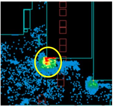
Figure 8: Congestion Map (before)
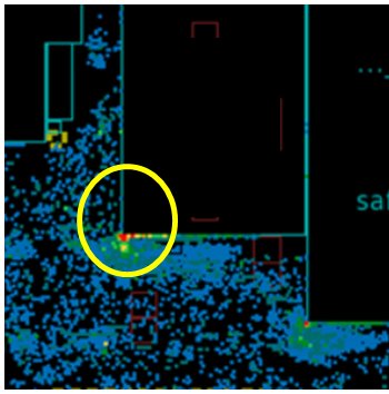
Figure 9: Congestion Map (after)
Above port reduction algorithm helped to find many such cases where I/O ports at partition level could be optimized. Feedback was shared with RTL designer and no of I/O ports on these two partitons were reduced from 10K to less than 6K. This gave floorplan designer enough margin to avoid need of placing I/O ports close to corners.
Using this ports reduction technique has nearly eliminated this corner congestion problem in that SoC.
5. Conclusion/Summary
SoC physical design hardening strategy is an important activity of any SoC development cycle.
Defining right physical partitions having correct size, shape and no of I/O pins helps big way to achieve goal of predictable and convergent timing closure cycle .
SoCs targeted for automotive applications have some unique constraints and hence conventional partitioning techniques could not always be working.
Defining clean physical partitions for auto chips is constrained by safety requirements and DFT logic to meet high coverage goals.
Our proposed algorithm helps designer to refine physical partitions which minimizes I/O ports at hard partition boundary by analyzing logical connectivity of interface logic.
Reducing ports helps to reduce overall routing congestion around partition boundary and achieve better timing results for interface paths.
