By Kurt Shuler (Arteris IP)
Abstract. The growth of artificial intelligence (AI) demands that semiconductor companies re-architect their system on chip (SoC) designs to provide more scalable levels of performance, flexibility, efficiency, and integration. From the edge to data centers, AI applications require a rethink of memory structures, the numbers and types of heterogeneous processors and hardware accelerators, and careful consideration of how the dataflow is enabled and managed between the various high-performance IP blocks.
This paper will define AI, describe its applications, the problems it presents, and how designers can address those problems through new and holistic approaches to SoC and network on chip (NoC) design. It also describes challenges implementing AI functionality in automotive SoCs with ISO 26262 functional safety requirements.
Keywords: Artificial Intelligence (AI), Machine Learning (ML), Dataflow, ISO 26262, Functional Safety, Semiconductor
1. The Evolution of AI
In reality, true AI is a long way off, but for now it is implemented using techniques such as machine learning (ML) based on convolutional neural networks (CNN) as a proxy. These technologies may end up as a subset in the AI of the future, or AI may follow a completely different path. Regardless neural networks are at the heart of current AI approaches (see Figure 1).
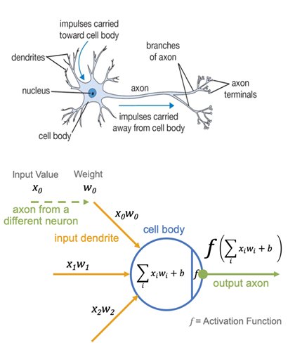
Figure 1: A brain’s neural networks (left) and their mathematical models (right) are the basis of current AI approaches. (Image source: MIT, Stanford)
In a neural network, single neurons receive an input signal from dendrites and produce an output signal along the axon. The signal interacts with the dendrites of other neurons via synaptic weights, represented by the variable “wx” on the right. The weight values are learned during the training and algorithm development process and they control the amount of influence that the input dendrite has on the neuron’s ability to “fire”. The ability of the neuron to fire is determined by the activation function (f), which is related to the sum of the input values times weights for each input dendrite: a value above or below a certain threshold causes an output signal on the output axon. The output axon then connects to a dendrite of a different neuron.
To form a neural network, many “cells” and their neurons connect to create an input layer, one or more hidden layers (the number of which determine the network’s “depth”), and an output layer.
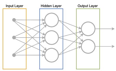
Figure 2: A feed-forward neural network typically comprises an input layer, a hidden layer, and an output layer. There is an ever-expanding array of neural network configurations, each seeking to optimize for efficiency and effectiveness for the various applications of AI. (Image source: Stanford)
In Figure 2, above, each circle is a neuron and an arrow represents connections between neurons. In the traditional feed-forward neural network shown, a hidden layer neuron is a neuron whose output is connected to the inputs of other neurons and is therefore not visible as a network output.
The weighted sum calculations described in Figure 1 propagate from left to right, including within the hidden layer(s), until the neural network provides its outputs.
2. Training and Application of AI
Mainly based upon its pattern-recognition capabilities, AI has found applications across many fields, from face recognition for security to financial transaction analysis to autonomous vehicles. However, before it can be deployed, extensive “training” must first take place using specialized hardware at the various data centers now available for developers. This can be an arduous, iterative, processing-intensive process where the exact weights are assigned to provide the correct output for a given input. However, there are publicly available data sets that ease the process. These are available from various universities or Google for typical applications as a road sign or animal recognition. The cleaner and higher the quality of the dataset, the better the algorithm and resulting output.
Once the model is finalized, it is typically mapped to an AI inference engine in the cloud or on the edge application device or system. The inference engine comprises dedicated hardware that takes incoming ambient data and runs the generated model against to classify objects, make decisions, and provide an output as efficiently as possible. It’s often possible to continually update the model on a remote device using scheduled updates, sporadic updates, or near real-time updates using over-the-air (OTA) connectivity to a data center.
Given the amount of development going into realizing the autonomous vehicle, this is an excellent example to use for the AI training process (see Figure 3).
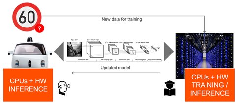
Figure 3: The autonomous vehicle shown here already has an inference engine running. The model is being updated at the data center as new data is acquired and the new model is then deployed to the vehicle in near real-time over a wireless connection. (Image source: Arteris IP)
In this example, neural networks are being used in the datacenter to train neural networks running on the car. There is specialized accelerator hardware in the data center to train the network, and customized hardware in the device that uses the trained neural net to classify objects. When the car experiences something that doesn’t make sense or is new, it sends the new data and associated driver action to the data center where the action to take in the presence of the new situation can be learned. The data center then updates the “weights” in the car’s neural network.
3. AI Hardware Requirements
For AI to work effectively in an autonomous vehicle or any other mission-critical application, it must have three critical dependencies:
- The accuracy and timeliness of the incoming data
- The reliability and efficiency of the AI models and the resulting algorithm
- The speed and efficiency of the underlying system hardware (including for sensors, control, and actuators).
AI mission-critical incidents require analysis, alerts, and directions and are only as useful as the response time. For example, an automotive ADAS or autonomous vehicle system is composed of multiple advanced sensors including LiDAR, radar, inertial measurement units (IMUs), and cameras, as well as pressure and temperature sensors and data connectivity for continuous uploads and downloads of surrounding conditions. The signal chain requires accurate detection and conditioning of sensor outputs, as well as reliable low-latency communications within the vehicle as well as between the vehicle and the surrounding infrastructure.
The vehicle-to-infrastructure (V2I) access across wireless networks demands sufficient bandwidth and quality of service (QoS) just to ensure the AI processing network gets the information it needs to make appropriate decisions.
Advances in 5G cellular networks are widely expected to meet the communications requirements. However, once acquired, the data must be processed, analyzed and sent back as actionable data or signal outputs to provide the required alerts or perform the necessary changes in vehicle direction or speed. Assuming the engineers have developed the most accurate models and most efficient AI algorithms, the next step is to ensure the fastest and most efficient hardware platform. This demands careful attention to processing performance and dataflow management.
For electric vehicles and other edge-based battery-powered applications the hardware must also be designed for power efficiency. This processing distribution brings up the concept of Fog Computing, whereby analysis of data is done at the most suitable point between the edge and the cloud. Factors that go into making this decision include latency requirements, available resources (CPU, memory, power), security concerns, and data dependencies, including information from other nodes in the wider network.
The decision as to whether or not to implement elements of Fog Computing is for the network or system architect, but in many ways the considerations are a macro version of those facing a NoC designer for SoCs, including:
- Optimum processing per milliwatt
- Data locality (buffers; cache coherence)
- Avoidance of bottlenecks through appropriate allocation of available bandwidth
- Functional safety, which depends upon both redundancy strategies as well as security (a system cannot be considered safe if it is insecure)
To accomplish this, the underlying hardware, whether in a data center, in the “fog”, or at the edge, should be able to perform parallel processing at a massive scale for model training. Depending on where the system resides, the SoCs may also integrate heterogenous processor approaches that incorporate CPUs, FPGAs, GPUs, and dedicated hardware processing cores, while also providing access to large amounts of low-latency memory.
4. AI driving semiconductor development
Managing the advanced hardware and developing the flexible on-chip interconnect and associated software for optimum dataflow is where much of today’s semiconductor research and development attention is being applied. Looking out to 2025, the real dollar growth for the semiconductor industry is in algorithm-specific ASICs, ASSPs, SoCs, and accelerators for AI, from the data center to the edge.
According to a report by Tractica, the upcoming change in focus will be so radical, that by that 2025 timeframe, a full five-sixths of the growth in semiconductors is going to be the result of AI (see Figure 4).

Figure 4: According to data from Tractica, by 2025 a full five-sixths of the growth in semiconductors will be the result of AI. (Image source: Tractica)
Much of this research will be going into finding the right mix of computing architectures to implement in chips to achieve the maximum performance in the data center and the optimum balance of computing power and efficiency at the edge (see Figure 5).
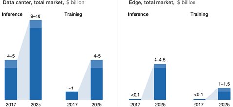
Figure 5: While the hardware for inference engines in the data center is expected to grow in absolute value to between $9 and $10 billion by 2025, the rate of growth of inference at the edge is more rapid, growing to from under $0.1 to between $4 and $4.5 billion. . (Image source: McKinsey & Company)
The projections are staggering: According to a January 2019 study by McKinsey, hardware for inference engines in the data center is expected to grow in absolute value from $4.9 billion in 2017 to between $9 and $10 billion by 2025. At the edge, the rate of growth of inference at the edge is also interesting, growing to from under $0.1 billion to between $4 and $4.5 billion.
To address this fiercely competitive market, especially at the edge, where low power low latency is critical design constraints, there are already a number of competing architectural approaches on the market from companies such as Nvidia, Mobileye (now part of Intel Corp.) and Movidius (see Figure 6).
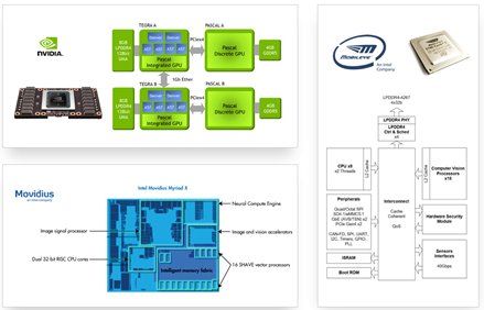
Figure 6: Competition to find the optimum AI processing foundation for the edge has resulted in a number of exceptionally efficient approaches from companies include Nvidia, Movidius, and Mobileye. (Image sources: Arteris IP, Nvidia, Intel)
A close look at the architectural approaches exposes a common thread: The SoC architectures are adding more and more types and numbers of hardware accelerators with each new version of a chip. In essence, the architects are slicing the algorithms finer and finer by adding more and more accelerators explicitly created to increase efficiency. There are also strategically placed islands of cache coherency as it’s tough to manage this data flow manually with many processing functions occurring simultaneously.
5. Managing Complex IP Blocks and Dataflow
As the types and numbers of processing elements have increased, interconnects and memory architectures connecting these elements becomes the critical path to success. So much so, that standard interconnects have given way to a highly specialized and efficient NoC approaches such as the FlexNoC® noncoherent interconnect and the Ncore® cache coherent interconnect (see Figure 7).
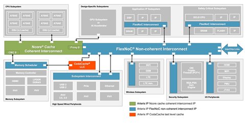
Figure 7: Both non-coherent and cache coherent NoC interconnect IP have emerged to better manage data flow, avoid bottlenecks, fix errors to ensure optimum performance. (Image source: Arteris IP)
For higher performance and flexibility, recently introduced CodaCache® standalone last level cache (LLC) IP supports dedicated, shared, and distributed partitioning, as well as on-chip scratchpad storage.
To bring cache coherency to current NoCs, it’s possible, as shown in Figure 8 on page 9, to integrate existing non-coherent processing elements into a cache coherent system using configurable proxy caches. The associativity, size and policy of each proxy cache can be optimized for use cases. In this example, the five hardware accelerators act as coherent peers to the two Arm CPU clusters. In addition, processing elements connected to a proxy cache can efficiently share data with each other using that cache.
There are at least two important use cases where it’s useful to use proxy caches to allow non-coherent IP to participate as fully-coherent peers in the coherent domain:
- Networking and storage: Lots of existing IP can be made coherent with the latest Arm processor clusters.
- Machine learning: Hardware accelerators for use within the data center for learning as well as in automobiles for classification.
6. Data flow protection for automotive ISO 26262 safety
Data flow efficiency is not the only challenge facing automotive architects. They must also be concerned about data protection to ensure the functional safety of the system. A well-developed NoC can play an important role here as it sees all the data transferred on the SoC. As such, it can both find and, in some cases, fix errors to improve the safety of the chip. It can also improve diagnostic coverage to meet requirements for ISO 26262 automotive functional safety and other safety and reliability standards (Figure 8).
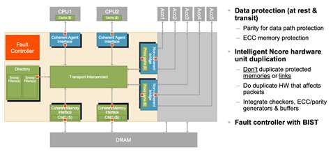
Figure 8: A well-designed NoC design goes beyond data flow management and cache coherency to allow non-coherent IP to participate as coherent peers to CPU clusters and for full diagnostic coverage to meet ISO 26262 requirements. (Image source: Arteris IP)
To meet to ISO 26262 requirements in on-chip hardware, two sets of techniques are implemented in Figure 8:
- ECC and parity protection: Implemented across all data portions of the chip having safety or reliability requirements. This protection is configurable.
- Intelligent hardware duplication: Done for the parts of the interconnect that affect the content of a packet. Is also configurable to meet diagnostic coverage goals tailored for the desired ISO 26262 automotive safety integrity level (ASIL).
In this case, both of these techniques do not impact performance and they are both integrated with automatically-generated ECC generators and data checkers. In addition, these safety mechanisms are automatically integrated with a configurable on-chip fault controller. This manages interconnect-wide BIST functions and communicates error status to runtime software.
Augmenting these features for automotive safety are the FlexNoC® and Ncore® Resilience Packages. These provide hardware-based data protection for increased SoC reliability and functional safety. Also, to help get designers up and running with functional-safety compliant IP, Arteris is working closely with ResilTech S.R.L. to create a set of deliverables which can be used as a starting point in the preparation of ISO 26262 work products.
7. Conclusion
AI is pushing the limits of SoC design in terms of performance and efficiency, so much so that it will play an increasingly important role in IC design and revenue for many years to come. As designers innovate with processing elements and memory architectures, it has become clear that the NoC has a unique role to play in ensuring that SoC data flow and data integrity are maintained.
In specific applications such as ISO 26262-compliant automotive systems, NoCs, innovative LLC caches, improved resiliency packages and even partnerships to provide designers with the support they need, are going a long way toward achieving what is becoming the ultimate test of AI: Fully autonomous vehicles.
Author
 Kurt Shuler is vice president of marketing and functional safety manager at Arteris with 20+ years’ experience in design IP, semiconductors, and software in the automotive, mobile, consumer, and enterprise segments, having served in senior executive and product management roles at Intel, Texas Instruments, ARC International and four technology startups. He is a member of the U.S. Technical Advisory Group (TAG) to the ISO 26262 TC22/SC3/WG16 working group, helping create automotive functional safety standards for semiconductors and semiconductor IP, and was one of the semiconductor design IP experts contributing to the writing of the new ISO 26262:2018 2nd Edition, Part 11, “Guideline on Application of ISO 26262 to Semiconductors”. He has extensive experience in aviation electronics operational testing, software quality process implementation, and functional safety mechanism requirements writing. Before working in high technology, Kurt flew as an air commando in the U.S. Air Force Special Operations Forces.
Kurt earned a B.S. in Aeronautical Engineering from the United States Air Force Academy and an M.B.A. from the MIT Sloan School of Management.
