By Invia
Why Implementing a Secure Boot in Your ASIC, SoC or FPGA?
The number of new viruses and malwares created every day is getting close to 1 million. Thus, in an always more connected world, getting protected against these attacks becomes absolutely critical.
To make a device trustable one needs to make sure it runs only genuine firmware. Let’s take the example of a portable connected electrocardiogram (ECG): if a hacker could install a malicious piece of software on this equipment, such software could lead to extremely severe consequences:
- Send the confidential patient data in clear over the air, making it accessible to anyone
- Report fake patient data leading to false alarms or wrong diagnosis
- Make the device stop measuring heartrate, this is often referred as a Denial Of Service (DoS) attack and could be life threatening
Secure Boot Principles
Using cryptographic digital signatures is the way to guarantee firmware authenticity and integrity.
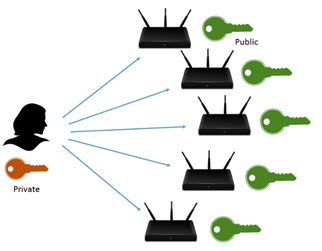
To implement digital signatures, asymmetric cryptography is often the preferred option. It allows an easy management of the keys. Asymmetric cryptography involves a key pair made of a private key and a public key. The private key allows privileged operations and must be strongly protected. The public key can be openly disclosed and is thus easy to distribute.

Figure 1. The Public key can be easily distributed as it is not confidential
Once the software development is complete, the developer generates a key pair that will be further used to authenticate the firmware. In order to enable secure boot, the firmware is signed with the private key by the developer and is verified with the public key in the end product.

Figure 2. Firmware signature happens in R&D facility using the private key

Figure 3. Firmware signature verification in the field uses the matching public key
At each boot, end equipment in the field will verify the firmware signature using the matching public key. The public and private keys are mathematically and uniquely linked. The principles of asymmetric cryptography are such that only the privileged entity (the developer in our case) can sign a content with the private key that he owns while any entity can check the signature using the public key. The main benefit of this approach is that one does not need a secret to verify that the firmware is genuine, hence there is no need to store a secret in the devices deployed in the field.
This method is widely used because of its flexibility, on the other hand it brings some constraints. Let’s now see what these constraints are and how INVIA’s software libraries or Intellectual Property blocks overcome them.
Invia provides the building blocks to efficiently support secure boot
Asymmetric cryptography operations are generally slow and call for a lot of computing resources. For a powerful CPU core at high frequency (e.g. Arm® Cortex A or Intel™ x86 running at 1GHz), the computation time of a digital signature can be considered as acceptable. When it comes to embedded processors it is a whole different story since a digital signature verification can take seconds. Because the boot time is often a critical parameter, increasing the boot time by several seconds is clearly not an option. The challenge of the slow computation for asymmetric cryptography can be solved by the integration of hardware cryptographic accelerators or by using a well optimized software library. Here follow some examples of ECDSA verification times based on NIST P256 curve:
| Arm® Cortex M3 CPU Core | Non optimized C code | Invia optimized assembly code | Invia hardware accelerator |
| Signature verification time (ms) @96 MHz | 500ms | < 190ms | < 50ms |
| Signature verification time (ms) @32 MHz | 1.5s | < 600ms | < 150ms |
Another way of reducing the signature verification time is to reduce the amount of data to be verified. Let’s assume we want to verify the digital signature of a 100kB piece of firmware. Assuming each verification operation lasts 200ms using ECDSA with 256 bits key length. ECDSA runs on 256 bits long blocks. The signature computation would be (100,000 x 8 / 256) x 0.02 = 625s . Once more we are in a situation that would be hardly acceptable and could get even worse if it comes to a full operating system which size would be in the MB range.
The way to circumvent this drawback is to substitute a digest to the original content (the firmware in our case). To make this substitution valid without introducing a security breach the digest must have the following properties:
- the same message always results in the same digest
- it is infeasible to generate a message that yields a given digest value
- it is infeasible to find two different messages with the same digest value
Such a digest is called a hash and the functions able to turn a digital content into a digest with the properties above are called Secure Hash Functions. In addition, hash functions are also designed so that a small change to a message should change the hash value so extensively that the new hash value appears uncorrelated with the old hash value. Speed of the hash computation is obviously a key factor too.

Figure 4. Hash based digital signature
Similar to ECDSA operations, hash can be very time consuming and here again dedicated hardware can also help improving boot performances. A DMA controller supporting transfers from the target firmware memory and the hardware hash accelerator may also improve performances.
| Arm® Cortex M3 CPU Core | Non optimized C code | Invia optimized assembly code | Invia hardware accelerator |
| Hash computation time (ms) @96 MHz for 100kB | 0.58s | < 0.25s | < 0.08s |
| Hash computation time (ms) @32 MHz for 100kB | 1.7s | < 0.75s | < 0.24s |
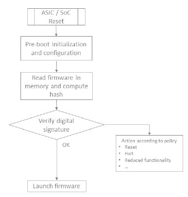
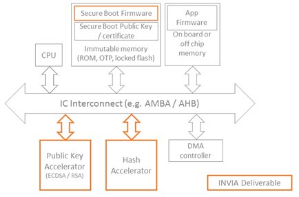
On top of the ECDSA and SHA hardware accelerators or libraries, the secure boot process shall be managed by a dedicated secure boot firmware. This secure boot firmware should be stored in an immutable memory, ideally in ROM or OTP and as an alternative in a locked flash sector along with the device public key certificate.

Figure 5. Typical secure boot sequence
Invia provides sample secure boot code supporting the sequence above as well as technical support for implementation in your target ASIC, SoC or FPGA.
Secure Firmware Updates Over The Air (FOTA )
To efficiently counter malware attacks, on top of supporting secure boot, it is also critical to guarantee the security of the firmware updates over the air.
The technique described above relying on firmware signature using a private key and verification based on a public key also applies to firmware updates and brings a high level of flexibility as it does to the secure boot.
Hence, same building blocks are used for secure boot and secure updates.
Conclusion
Secure boot is fundamental when it comes to design a trusted electronic device. Asymmetric cryptography offers the highest level of flexibility but also sets some challenges when it comes to implementation in embedded systems. INVIA software and hardware IPs provide proven and efficient solutions in terms of cost, resistance to attacks and performances.

Figure 6. Building blocks for secure boot implementation
