By Sonia Sharma, eInfochips (An Arrow Company)
ABSTRACT
At times physical design engineers find it difficult to relate with the additional timing modes introduced in PnR due to DFT insertion. These additional timing modes and related issues could be handled more efficiently if we understand why a scan chain is needed and how it works.
1. INTRODUCTION
Chips without DFT implementation will mostly have only one timing mode of operation and hence just one timing mode in implementation (Place and Route) - functional mode (some others may call it as system mode). When DFT is inserted in a netlist, more timing modes come in to the implementation flow - like Shift, Capture, Scan, Bist
Sometimes physical design engineers find it difficult to understand the scan chains and its impact on the physical design.
2. SCAN FLIP FLOP : BASIC BUILDING BLOCK OF A SCAN CHAIN
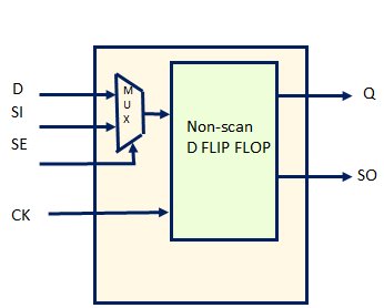
The basic building block of a scan chain is a scan flip-flop. A scan flip-flop internally has a mux at its input. SE (enable signal for mux) determines whether D (functional input) or SI (test input) will reach to the output of the flip-flop when active clock edge comes at CK.

Figure 1. scan - D FLIP FLOP
3. SCAN CHAIN
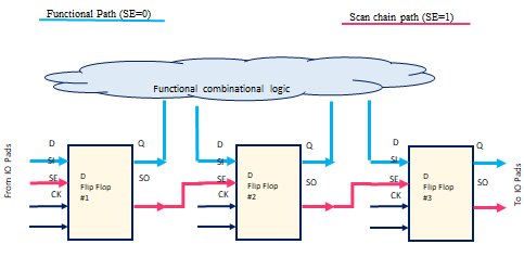
All the flip-flops present in the design are replaced with the scan flip-flops (for a full scan design). The scan flip-flops are connected together in form of a chain – scan chain.
Scan chain acts as a shift register when the design is in test timing mode; SE (test enable signal) is active. The first flip-flop of the scan chain is connected to the scan input port and the last flop the scan chain is connected to the scan output port.
When some of the flip-flops are deliberately not converted to scan flops, such designs are called partial scan design. Making a design full scan makes the design more testable for manufacturing defects at the cost of complexity, area and power.

Figure2. Scan chain
4. NEED FOR A SCAN CHAIN IN THE DESIGN
Scan chains are used to detect manufacturing defects present in the combinational logic of the design. ATPG tool generates the test patterns in such a way that all the nodes present in the combinational logic are sensitized and verified for manufacturing defects.
5. FUNCTIONING OF A SCAN CHAIN
There are three stages of scan chain operation –
-
Scan In
Objective - test patterns are loaded keeping the design in test timing mode -
Capture
Objective - Design is kept in functional timing mode and test pattern response is captured -
Scan Out
Objective – Design is brought back in test timing mode and test pattern response is unloaded (at times, this operation simultaneously initiates the injection of next test pattern via Scan In)
Stuck-At testing is done at a slower frequency hence a single clock capture pulse is sufficient for this. While Path Delay or Transition faults testing is done at functional speed (at speed testing) therefore the design is put in the function timing mode at functional frequency. This will require two functional clock pulses in the capture mode.
We can say, the capture timing mode execution for a scan chain is slightly different for slow capture (for Stuck-At faults) and at speed capture (for Path Delay or Transition faults). Let us understand it in detail during capture stage discussion.
5.1. Scan In Stage
The objective of this mode is to load the correct test vectors and therefore it is called as loading stage.
In this mode, SE is kept high (asserted) so that the scan flip-flop sees only SI as an input. This means all combinational logic present between the flip-flops are bypassed. The test patterns will flow SI to SO and from SO to SI of the next flip-flop. This will form a chain and will act as a shift register.
The test patterns will serially enter from the scan input port; to the first flip-flop of the scan chain and then at each active clock edge, it will shift to the next stage of flip-flop (shift register behaviour) and so-on. This way all scan chain elements will be loaded with the correct test patterns. (Please refer Figure3)
If there are n flip-flops in a scan chain, then after n-1 number of clock cycles test vectors would reach at the SI (Q) pins and hence at the corresponding combinational logic between the flip-flops.
This is called the loading of test patterns.
5.2 Capture@Slow-Stuck-At
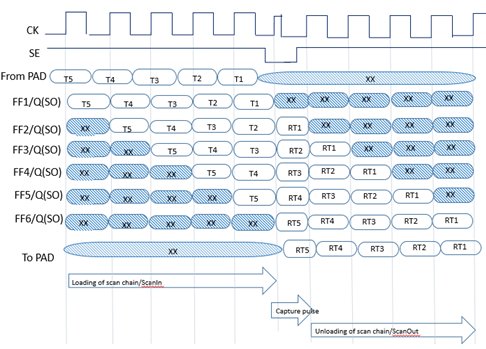
Capture is run at a slower frequency to detect Stuck-At faults. This mode remains active just for one clock cycle. During this mode, SE (enable signal) is de-asserted so that the flip-flops works in normal functional timing mode and the test pattern response processed by the combinational logic is captured at the next stage of the flip-flop.
Before arrival of next active clock edge, the test pattern response is processed by the combinational logic and becomes available at the D input of next flip-flop. As soon as the active clock edge arrives, the processed test pattern response is captured by the next flip-flop and becomes available at the Q and SO pin. (Please refer Figure4)
5.3. Capture@AtSpeed-Transition/Pathdelay
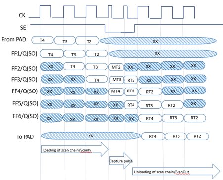
Capture is run at functional frequency to detect Path delay or transition faults. For at speed testing, capture mode remains active for two clock cycles since launch and capture both have to be at speed. During this mode, SE (enable signal) is de-asserted so that the flip-flops work in normal functional timing mode.
Pattern generation is complex for this testing, as it requires taking care of two flip-flop stages. First capture pulse launches the test pattern to the targeted combinational logic and the second pulse captures the test pattern response at the functional frequency.
During the first capture pulse the test pattern data is launched from D to Q pin of the flop (hence to the targeted combinational logic) and during the second capture pulse it is captured by the next flip flop and reaches to the Q and so SO pin of the subsequent flip-flop in the scan chain. This way the test pattern response is generated and captured at functional frequency. First clock pulse is launching the test pattern to the targeted combinational logic and second clock pulse ensures that combinational logic is getting at speed processing time. (Please refer Figure5)
5.4. Scan Out
This is also called the unloading of the scan chains. SE (test enable) is again asserted in this mode, which brings the design back in test timing mode. At each active clock edge, the captured data (test pattern response processed by the combinational logic) is serially shifted out on the scan chain.
In this mode, the test pattern response captured at the SI pins of the flip-flops is shifted serially out to the scan output port to crosscheck it with the expected results.

Figure3.

Figure4. Waveforms for Stuck-At Capture

Figure5. Waveforms for At-Speed Capture
6. ADDITIONAL TIMING MODES IN PnR DUE TO SCAN CHAIN INSERTION
As we have discussed earlier, chips without DFT implementation will mostly have only one timing mode of operation and hence just one timing mode in implementation (Place and Route) - functional mode or system mode. When DFT is inserted in a netlist, more timing modes coming in to the implementation flow - like Shift, Capture, Scan, Bist. (Please refer Section 1)
We have also discussed, a scan chain has three stages of operation – scan-in, capture, and scan-out. (Please refer Section 5)
In general, Scan-In and Scan-Out operations are modelled as Scan Shift timing mode in the PnR (implementation) whereas Capture operation is modelled as Capture timing mode.
We have observed that all functional combinational logic is bypassed for Scan-In and Scan-Out operations hence Scan Shift timing mode is always critical on hold timing checks for the flops. On the other hand, Capture operations involve combinational logic and executed at functional frequency therefore capture-timing mode is critical on setup timing checks.
7. PROS AND CONS OF A LONGER SCAN CHAIN
7.1. Pros
Since one chain has more number of elements so, the total number of scan chains in the design would be lesser. Therefore, lesser number of scan input and scan output ports will be required.
Number of IO ports required for Scan Chains = 2 X number of Scan Chains
7.2. Cons
More clock cycles are required during Scan In and Scan Out operations
Number of cycles required for a ATPG pattern = Number of flip flop in the longest scan chain
8. SCAN MODE IS OPERATED AT A LOWER FREQUENCY WHILE IT IS EASY TO ACHIEVE HIGHER FREQUENCY FOR SCAN TIMING MODES
It is easy to achieve high frequency for the scan timing modes.
Since all functional combinational logic between the flip-flops is bypassed in the scan timing modes, it becomes easy to meet the setup requirements. Hence, higher frequencies can easily be achieved for DFT timing modes.
Higher is the frequency of scan timing mode, more patterns can be shifted in a given amount of time so testing time will be reduced so it will save the cost.
Still these timing modes are never operated at higher frequencies?
Togging is very high in the Scan timing mode. Almost all the flip-flops (as well as the combinational logic between the flip-flops) are toggling. This will lead to huge dynamic power loss. Huge amount of current is drawn from the supply leading to extreme voltage drop and heating.
The chip will not be able to sustain at higher frequencies due to excessive voltage drop and heating in the scan mode.
Though it is easy to achieve higher frequency in the shift timing mode, still this timing mode is operated at a much lower frequency (In general <=10 MHz)
At the same time, keeping the frequency too low would increase the tester time and hence the cost of the chip.
CONCLUSION
Insertion of scan chains in the design leads to additional cost in terms of area, speed, power, design- cycle, complexity. Scan chains are inserted to serially shift in the test patterns and serially shift out the test pattern responses. This additional cost is indispensable because it ensures that every node in the design becomes controllable and observable and therefore testable.
ACKNOWLEDGEMENT
The author would like to thank eInfochips company for providing the access to required resources.
REFERENCES
-
“Principles of testing electronic systems”, Sami Mourad & Y. Zorian
-
“Essentials of Electronic Testing for Digital, Memory and Mixed-Signal VLSI Circuits”, Michael B Lee & Vishwani Agrawal
-
“VLSI Test Principles and Architectures: Design for Testability”, Cheng-Wen Wu, Laung-Terng Wang, and Xiaoqing Wen
