by Imed Moussa and Thierry Roudier
TNI-Valiosys France
Email : {imed.moussa, thierry.roudier}@tni-valiosys.com
Tel : +33 4 76 18 17 45
Fax : +33 4 76 61 93 93
Abstract:
Most of system on chip (SoC) being designed today could reach several millions of gates and more than 2 GHz operating frequency. In order to implement such system, designers are increasingly relying on reuse of intellectual property (IP). In order to effectively re-use an IP in a system chip, a set of abstracted models of the IP must be provided that enable the complete design and verification of the system chip that instantiates the IP. This work addresses the main issues in SoC design, namely the system design methodology, system level modelling, and IP integration for platform based design. The methodology presented allows the reuse and the integration of IP components at any level of the design process, using IP modelling methodology. At each stage, the system functionality and its characteristics can be evaluated and validated. In this way, IP modelling presents a number of unique technical challenges. This paper discusses these challenges and offers a new methodology approach for IP modelling during system level design flow.
1. Introduction
The integration of complex components, which are pre-designed and well tested, drastically reduces the design complexity and, thus, saves design time and allows a shorter time to market. Since the idea of IP reuse promises great benefits, it must become an integral part in the system design methodology[1]. Furthermore, the use of IP components must be directly supported by the design models, the tools and the languages [2][3] being used throughout the design process. For example, it must be easy to insert and replace IP components in the design model (``plug and - play''). Today’s standard SoC integration mechanism makes use of IP connected directly to a standard bus. There are several problems related to this approach. By connecting the IP directly to the bus, the IP interface must be modified to fit the particular bus being used, and the particular system in which the core is being used. Having to adapt the core to each particular bus and system and reuse a particular IP core from system to system, is totally out of date. Time to market is too important. Consequently, the interest grows up for a standardization of the IP interfaces (registers, memory maps and black box interface) and for an automatic generation of the communication drivers between the IP and the standard bus.
The main objective of our approach is to provide a valuable environment in which designers can investigate system bandwidth and performance requirements[4]. This “user-friendly" environment allows for an easy connection of IPs to any standard SoC Bus, and at any level of abstraction. These levels are: the functional, the unitmed transactional, the timed transactional, the Bus Cycle Accurate (BCA), and the Register Transfer Level (RTL).
2. On Chip Bus Architecture
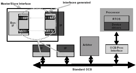
Figure 1 illustrates a typical architecture of a system on chip bus. This architecture is composed mainly of standard bus, processor, and several IP components. For the IP integration, the key issue is the hardware and software interface generation.

Figure 1: On Chip Bus architecture
HW/SW interface generation is one of the most important and sensitive parts of the path to the implementation of System On Chip (SoC) design. It includes both the automatic generation of the HW parts of the interface (mainly bus interface) and the corresponding software drivers. Interface generation is a hierarchical process that starts with communication and protocol layers generation. For this reason, communication techniques used at the different levels offer also interesting perspectives to encapsulate virtual components.
In this section, a special emphasize will be put on the interface generation between the IP and standard SoC bus such as the AMBA bus or the ST-bus. This interface consists of two parts: software part and hardware part. The hardware part is in charge of handling the communication between the bus and the IP interface registers. The software part provides the automatic generation of the software drives related to: a targeted commercial Real Time Operating System (RTOS), and to a specific processor such as the ARM or the Power PC.
In order to create a repeatable process for IP integration and interface generation, we consider implementing a standardized design flow that allows to define and integrate the IP models at different abstraction levels of communication defined in the next sections. At the high level, the architecture is made of a backbone bus and a software IP communicating through channels. At the RTL level, the channels will be mapped to communication interfaces described as it is shown in figure1.
The design methodology proposed lets the designers separate the functional behavior of the IP from the communications. This makes swapping out from one IP to another much easier. It also allows the designers to quickly evaluate the potential of an IP versus another.
3. Abstraction Level Models
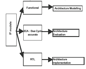
As already stated in the previous section, in order to effectively re-use a hardened IP in a system chip, a set of abstracted models of the IP must be provided that enable the complete design and verification of the system chip that instantiate the IP. The models provided must form a complete set of deliverables for the IP and should enable the end user to easily and accurately integrate the IP in the system chip. Three IP model are used in our approach as it is shown in figure 2. First, At the system architecture, the IP is model at the functional level, that means that all the specifications such are the number of registers in the IP are known and these parameters are essential for architecture implementation. Second, the Bus cycle accurate model which is used for the architecture evaluation. And the third model is the RTL model on which all the parameters specified at the functional model are used for the architecture implemented.

Figure 2: IP Models
3.1 Functional Model
The functional level is the first step in the design flow [6]. It is used for the algorithmic evaluation and validation. In this environment, a pure software model is sufficient. This level has to be seen more as a specification output than an analysis environment. At this level, the functionality is implemented as stand alone model in ANSI C. In addition, the functional model should be portable across simulation environments by avoiding simulator specific constructs and interfaces.
3.2 Bus Cycle Accurate level
This level defines accuracy in terms of bus interface (equivalent to the RTL model). Processes may contain behavioural (un-timed) code. Communication links are mapped to physical busses in the architecture. At this level, we can perform a functional validation and a system analysis in terms of number of bytes transferred, throughputs, occupancies and latencies for each IP and for the common memory. But at the difference with the previous model, measurements will be close to the reality.
3.3 Register Transfer Level
Fully clock cycle accurate code. This is synthesisable code, which can be synthesised with standard RTL synthesis tool. At this level, two major alternatives are available: the first one consists of performing co-verification using ISS for the software part of the system, and the HDL simulator (or hardware emulator) for the hardware part as it is shown in figure 2. The second alternative consists of system implementation. In this case, we can perform RTL synthesis for the hardware part including FPGA mapping or ASIC implementation, and device drivers synthesis for the software part as it is shown in the fourth section of the paper.
4. Platform Architecture and Methodology
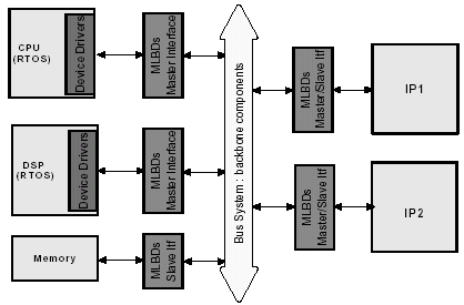
Figure3 illustrates a view of our platform based design approach. It consists of a system bus (STbus, AMBA, Sonics...) centric approach [5]. The architecture is composed of a SoC bus, and several components including hardware IPs, memories, and processors such as CPUs and DSPs. These processors may contain software IP processes which communicate with the system using software drivers. The blue boxes are the components/bus interfaces used to handle the communication inside the SoC. The communication interfaces is based mainly on two different technologies[7]: the first one called High Level Bus Drivers (HLBD) and the second one is the Low Level Bus Drivers (LLBD) or the HW/SW interfaces synthesis. We used in Figure 2 a generic name for these two technologies called Multi Level Bus Drivers (MLBD). This later can be implemented as HLBD or LLBD, depending on the level of abstraction. The HLBD are defined for the highest levels of abstraction (Untimed, Timed and BCA), whereas the LLBD concern the RT level.

Figure 3: Platform based design architecture based
The architecture in figure 3 is composed mainly of the different IP associated with their master or slave interfaces; the global memory which is consider in this architecture as a slave and that’s why we have a slave interface because the memory is used only to write data from the IP or from the processor in order to be read by another IP or the processor. The processor is considered of course as master. This processor is associated with its processor core, the RTOS and the IO drivers. And we have the on chip bus OCB backbone or arbiter which plays a central role in this architecture for handling the communication between all the components of the system through the bus.
4.1 Master drivers
Master drivers perform the communication between the system bus and architecture components defined like masters in the application. The drivers are globally unchanged from a level of abstraction to another. It will be interesting to understand the heterogeneity among communication paths : indeed, we consider that only the bus communication processes (bus layer) may be involved by a transition of communication level. This means that for a BCA level, the bus layer gives a BCA accuracy whereas the IP layer (IP communication side) keeps a transactional level.
4.2 Slave drivers
Slave drivers perform the communication between the system bus and slave parts of some architecture IPs and specific slave components (the system memory block for instance). The drivers are globally unchanged from a level of abstraction to another. As master drivers, only the bus layer may be involved by such a transformation.
4.3 IP Modeling Flow
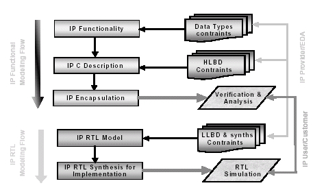
Figure 4 gives a brief idea regarding the IP modelling flow as well as the interaction between the IP user and the IP provider during the system design flow.

Figure 4: IP modelling flow for system design
One of the key techniques used in the design flow is the modeling of the system at the transactional level. Transactional level modeling is simply a high abstraction level for modeling. System model in RTL are concerned about the hardware details such as pin-level behavior of their system. With transaction level model it is possible to accurately model many aspects of as system at higher (read, write) level. During this transaction we will introduce a transaction as simple bus transfer. By using transaction model we simplifying the modeling effort and we also gain simulation speed.
5. Conclusion
In this paper we have presented a new methodology for IP modeling and reuse using standard system on chip bus. Our approach allows for an efficient way for IP integration and hardware software interface generation. In order to create a repeatable process for IP integration and interface generation, we have implemented a standardized design flow that allows to define and integrate the IP models at different abstraction levels of communication defined in this paper. At the high level, the architecture is made of a backbone bus and a software IP communicating through channels. This allows for an early high level architecture evaluation and analysis and thus meeting time to market constrains.
[1] Reinaldo A., Bergamaschi, and William R. Lee. Designing System-on-Chip Using Cores. DAC 2000, Los Angeles California.
[2] Peter L. Flake, Simon J. Davidmann, David J. Kelf, and Christan Burisch. The IP Reuse Requirements for System Level Design Languages. International Property 2000 Conference, Santa Clara, CA, April 2000.
[3] Jon Connell. Early Hardware/Software Integration Using SystemC 2.0. Class 552, ESC Francisco 2002.
[4] Michael Keating (Sysnopsys, Inc.) and Pierre Bricaud (Mentor Graphics Corporation) : "Reuse Methodology manual for system-on-chip designs".
[5] Wolf-Dietrich Weber. CPU Performance Comparison: Standard Bus Versus Silicon Backplane. Sonics Inc., White paper 2000.
[6] John Biggs and Alan Gibbon: Reference Methodology for Enabling Core Based Design. European Synopsys User Group, SNUG, Marsh 2002.
[7] Thierry Roudier, Imed Moussa and Philippe di Crescenzo : " IP Modelling and Reuse for System Level Design " published for DATE 2003
