By Shailesh Kumar, Jaya Patel, Meetu Sharma, and Rajendra Pratap Singh (eInfochips (An Arrow Company))
ABSTRACT
As chip size decreases the standard cell density and routing density of the design increases, due to that metal routes may interact with each other and it may result in a coupling effect which is known as crosstalk. It affects both signal nets as well as clock nets. In this paper, we would analyse the causes of high crosstalk delta delay on clock nets and find an automated way to take care of the crosstalk delta by applying single-width double-track NDR on clock nets at an early stage of the design cycle.
KEYWORDS
Standard cell, coupling effect, delta delay, NDR, crosstalk.
- INTRODUCTION
The design process of a chip plays a very important role in any device. There are three things that we have to optimize on a chip, they are Power, Performance, and Area.
The power consumption on a chip should be as low as possible, performance should be high and mostly a smaller area is preferred. As we go for the lower technology node, the lateral capacitance between two nets in a chip dominates than interlayer capacitance. Hence, capacitive coupling formed between two nets is the main reason for the functionality failure of a chip. Crosstalk is one of them.
If any logic is transmitted through a net that affects another neighbouring net due to capacitive coupling is known as crosstalk. It depends on coupling capacitance between two neighbouring nets, greater the coupling capacitance greater will be the crosstalk. It is an undesirable effect.
Crosstalk effects are mainly of two types: glitch and crosstalk delta delay. If the input of any combinational circuit changes due to that we get the unwanted transition at the output which is known as a glitch.[1] It is of two types: -
- Rise glitch
- Fall glitch
Aggressor driver switching from logic ‘1’ to logic ‘0’ and victim driver input being at steady state of logic ‘1’, due to that rise glitch can be observed at victim net as shown in figure 1.
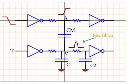
Figure 1. Rise glitch
If the input of the aggressor driver switches from logic ‘0’ to logic ‘1’ and victim driver input is at steady-state logic ‘0’, due to that fall glitch can be observed at the victim net as shown in figure 2. Spacing between aggressor and victim net and drive strength of the driving cell are the two parameters that affect the glitch.
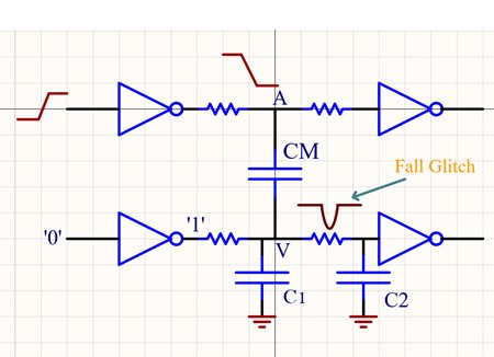
Figure 2. Fall glitch
If both aggressor and victim nets are close to each other, the value of coupling capacitance will increase that can lead to crosstalk. In the case of drive strength, more the value of drive strength more will be the glitch height, so we have to take care of these two aspects while routing. In case of crosstalk delta delay both aggressor and victim nets are switching and that impacts the delay of the cell. Here two types of switching can take place.
- Aggressor and victim nets switching in the opposite direction.
- Aggressor and victim nets switching in the same direction.
If both are switching in the opposite direction, the aggressor switches from logic ‘0’ to logic ‘1’and victim net switches from logic ‘1’ to logic ‘0’ refer figure 3. In this case, we can see the bump at the victim net and that bump depends on the coupling capacitor. Larger the value of the coupling capacitor larger will be the bump. This bump also affects static timing analysis of the circuit. The delay of the chip changes due to that latency also changes, which leads to setup timing violation.[3]
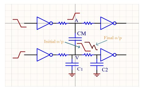
Figure 3. Aggressor and victim switching in the opposite direction.
If both nets are switching in the same direction refer to figure 4, then the delay of the victim net will reduce and the transition becomes sharper, which leads to hold timing violation.[4] In this paper, we will analyze the causes of high crosstalk delta delay on clock nets and find an automated way to take care of the crosstalk delta delay at the early stage of the design cycle. The experiment was done in ICC2 tool and crosstalk delta delay was calculated in PrimeTime.

Figure 4. Aggressor and victim switching in the same direction.
2. PROPOSED METHODOLOGY
After analysing the report of crosstalk delta delay generated by PrimeTime tool and nets which were having high crosstalk delta delay, it was found that in this design, most of the crosstalk delta violations were on sink clock nets that were connected to the clock pin of memory and length of those nets are more than 100um. In default PnR flow, single width, and double track Non-default routing rule (NDR) has been applied on root and internal clock nets.
However, on sink clock nets default routing rule has been applied i.e. single width and single track to save the routing resources. Based on this analysis, we have come up with one solution i.e. to apply single width and double track Non-default routing rule on sink clock nets connected to memory’s clock pin and having length of more than 100um.
WORKFLOW
The basic flow diagram of the experiment is shown in figure 5 and figure 6. The workflow can be divided into the below steps. Figure 5 shows the general flow of the physical design in which NDR applied to extracted nets before running clock tree synthesis. Figure 6 shows the detailed explanation of the NDR and their application on the clock nets.
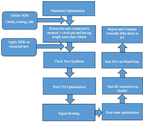
Figure 5. The basic flow diagram of the workflow
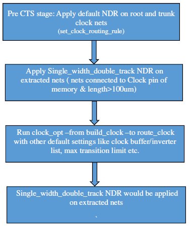
Figure 6. Applying NDR on clock nets
The difference in the clock net’s routing in the design with and without applying NDR on extracted nets is shown in figure 7 and 8. The routing in both cases is different.
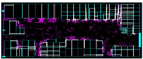
Figure 7. Routing of clock nets with a default flow
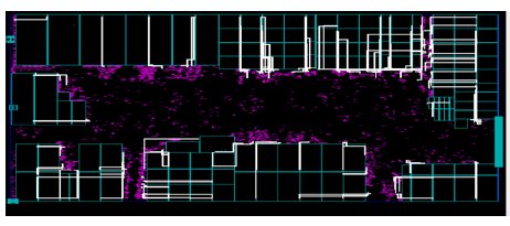
Figure 8. Routing of clock nets after applying NDR on extracted net
2.1 IMPLEMENTATION OF THE EXPERIMENT
The experiment has been implemented in design using ICC2. The technology node was 40nm. Then crosstalk delta delay has been checked in PrimeTime. Detailed implementation of the experiment is mentioned below:
- Perform Floorplanning, placement, and placement optimization.
- Extract the nets connected to memory’s clock pin and having length more than 100 um by a TCL script.
- Apply single width and double track non-default routing rule on those nets and default routing rule i.e. single width and single track will be applied on other sink clock nets.
- Perform Clock tree synthesis, post-CTS optimization, routing and post-route optimization.
- Run StarRC for the parasitic extraction
- Run PrimeTime and check the crosstalk delta delay.
With default flow:
- Routing of victim net (Sink_net_1) having the worst crosstalk delta delay is shown in figure 9.
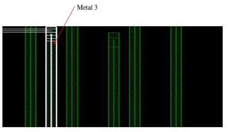
Figure 9. Worst crosstalk delta delay in clock net
After the implementation of the NDR before the clock tree synthesis, the result of the same clock net is different.
- Routing of the same net (Sink_net_1) is shown in figure 10.
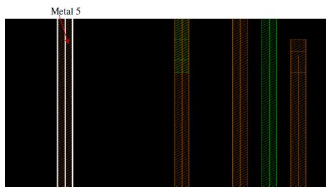
Figure 10. Improvement in clock net routing after NDR
3. RESULT
The total number of victim nets in the default flow is 321. The crosstalk delta delay of the top ten violating nets with their length is shown in table 1.
Table 1
| Net_name | Net_length(um) | Crosstalk_delta_max(ns) | Crosstalk_delta_min(ns) |
| Sink_net_1 | 303.2110 | 0.0000 | -0.104150 |
| Sink_net_2 | 264.2910 | 0.073034 | -0.073712 |
| Sink_net_3 | 202.8640 | 0.047006 | -0.046385 |
| Sink_net_4 | 231.2360 | 0.033836 | -0.036404 |
| Sink_net_5 | 312.3380 | 0.023931 | -0.036985 |
| Sink_net_6 | 216.5460 | 0.010246 | -0.034793 |
| Sink_net_7 | 196.4480 | 0.019085 | -0.031466 |
| Sink_net_8 | 209.6950 | 0.027458 | -0.029576 |
| Sink_net_9 | 206.3540 | 0.000000 | -0.029089 |
| Sink_net_10 | 174.7880 | 0.017201 | -0.028187 |
Table 2 represents the number of crosstalk delta delay after implementing the experiment. Here we observe that the total number of victim nets has been reduced to 189.
Table 2
| Net_name | Net_length(um) | Crosstalk_delta_max(ns) | Crosstalk_delta_min(ns) |
| Sink_net_1 | 314.7090 | 0.0000 | 0.0000 |
| Sink_net_2 | 270.8220 | 0.000073 | -0.007326 |
| Sink_net_3 | 200.4540 | 0.000 | 0.000 |
| Sink_net_4 | 235.7650 | 0.032421 | -0.036356 |
| Sink_net_5 | 275.2600 | 0.0000 | -0.012946 |
| Sink_net_6 | 280.2030 | 0.000 | 0.0000 |
| Sink_net_7 | 169.8410 | 0.000968 | -0.012191 |
| Sink_net_8 | 202.7020 | 0.0000 | -0.008138 |
| Sink_net_9 | 227.4800 | 0.008268 | -0.021662 |
| Sink_net_10 | 179.7020 | 0.006678 | -0.009295 |
Figure 11 shows the design and the routing of the clock net having crosstalk at the route optimization stage with default PnR flow. In the same design, we see the different routing of clock net after implementation of the experiment as shown in figure 12.
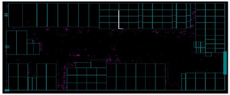
Figure 11. Routing of clock net before NDR
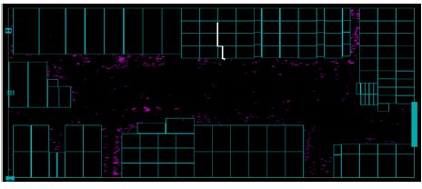
Figure 12. Routing of clock net after applying NDR
4. CONCLUSION
In lower technology nodes, we see a huge impact of crosstalk delay and crosstalk noise. This will lead to critical timing violations in the tape-out phase. If this crosstalk is on a clock signal, it will be even more critical to fix timing violations immediately since the changing of routing for the clock can lead to more timing violations later. To overcome this effect, we propose an automatic way to take care of crosstalk delta delay at the early stage of chip designing.
As the crosstalk was on clock nets, it would be critical to fix/reduce it manually at a later stage because any change in routing for the clock may lead to timing violations. We implemented this experiment on two designs. After the implementation of this experiment, the worst crosstalk delta delay and no. of violations have been reduced. Hence, we achieved crosstalk improvements regarding the number of victim nets and worst crosstalk delta delay.
REFERENCES
[1] A. Vittal, L. H. Chen, M. Marek-Sadowska, K. P. Wang, and S. Yang, “Crosstalk in VLSI interconnections,” IEEE Trans. Comput. Des. Integr. Circuits Syst., 1999, doi: 10.1109/43.811330.
[2] P. Heydari and M. Pedram, “Capacitive coupling noise in high-speed VLSI circuits,” IEEE Trans. Comput. Des. Integr. Circuits Syst., 2005, doi: 10.1109/TCAD.2004.842798.
[3] J. Bhasker and R. Chadha, Static timing analysis for nanometer designs: A practical approach. 2009.
[4] T. Stoehr, M. Alt, A. Hetzel, and J. Koehl, “Analysis, reduction and avoidance of crosstalk on VLSI chips,” in Proceedings of the International Symposium on Physical Design, 1998, doi: 10.1145/274535.274566.
Authors
Shailesh Kumar
He is a Physical Design Engineer in eInfochips working in the backend design domain. He holds master’s degree in Electronic System & Communication from National Institute of Technology, Rourkela.

Jaya Patel
She is a Physical design Engineer in eInfochips working in the backend design domain. She holds bachelor in technology degree in Electronics and communication from Nirma University, Ahmedabad.

Meetu Sharma
She is a devoted Technical manager in eInfochips with an experience of more than 16 years in ASIC.

Rajendra Pratap
He has completed his studies from Indian Institute of Technologies, India. He started his career with Motorola. Presently he is working as a branch manager in eInfochips (an Arrow Company). He has experience of over 22 years in ASIC.

