By Saumil Modi , Parth Kadiya (eInfochips, an Arrow company)
Abstract
With the increasing complexity in design in the semiconductor industry and advanced lower technology nodes, it is important as a DFT architecture design and service engineer to signoff the chip with timing simulation for all sets of the patterns generated by ATPG tool before it goes for manufacturing. To ensure a shorter and right Time-to-Market, it becomes increasingly necessary to debug timing mismatches for Scan patterns faster, if they exist. For larger designs, it becomes more difficult to find out particular failing cells response where we using high Compression ration as per complexity of the design. To find out the cells that are causing failures in VCS simulation, we have a unique feature supported by Tetramax ATPG Tool to generate the testbench with PSD flow and simulate that testbench in VCS simulation tool to find out the particular failing cell hierarchy.
We can generate the patterns and simulate with both Max testbench and Unified STIL flow. The patterns generated by Unified STIL Flow has limited support to debugging Parallel Simulation Failures. The typical Unified STIL Flow debug report lists the pattern number, scan output pin, and the shift index for each failure, but it does not include the particular scan cell during comparison for expected and golden output, not the cell that caused the failure. However, for parallel simulation pattern debugging, you usually need to identify the exact failing scan cell and instance name. The PSD flow approach for debugging parallel mismatches reduces the debugging time and efforts by giving the strobe failures.
Introduction
In the process of Design for Testability (DFT) Architecture, we insert logic and build the scan chains by replacing sequential elements into scan cells. This process further helps us to deal with manufacturing defects that occur due to fabrication issues in the design. Moreover, after successful insertion of scan chains, we perform ATPG that develops a set of test vectors. However, we need to run the design against a set of predefined stimuli (ATPG Test Vectors) and check (validate) the design response against an expected response. This process mimics the behavior of the tester against a device under test. There are chances that we face mismatches in the design response. The mismatches can result due to reasons like Incorrect or Incomplete STIL data, Incorrect Connections of the device to this stimulus in this testbench and Incorrect device response due to structural errors or timing problems inside the design. The only evidence of failure is a statement generated during the simulation run that indicates that the expected state of an output generated by ATPG differs from the state indicated by the simulation. Unfortunately, there is minimal feedback to help you identify the cause of the situation.
However, analyzing simulation-identified mismatches of expected behavior during the pattern validation process is a complex task. With the advanced technology nodes, the designs are becoming complex and therefore the debugging of pattern failure becomes very tedious. Especially debugging the 0/1 mismatches makes it more difficult if we do not have a waveform of the corresponding design where simulation is passing.
The set of patterns generated are generally chain patterns, serial patterns, and parallel patterns and we need to simulate all of them to validate the design response. We generate parallel patterns simulation in order to reduce the runtime for huge designs. In this paper, we will describe a flow to debug mismatches encountered during simulation and locate all the corresponding failures for each mismatch. The simulation using PSD flow needs to be done in parallel, but can also be used to debug serial simulation mismatches. This debug capability is an enhancement to the existing unified STIL flow (USF) and includes interoperability between TestMAX ATPG, MAX Testbench, and VCS.
The existing USF has limited support for debugging parallel simulation failures. The USF debug report lists the pattern number, scan output pin, and the shift index for each failure, but it does not include the information of failing cells during comparison of golden and expected output. To improvise on the existing USF we introduce PSD flow that does not only provides all the information present in USF flow but also includes the strobe failure provided the failed scan chain and scan cell information.
Debugging Parallel Mismatches with PSD FLOW

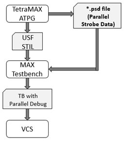
Figure 1: PSD Flow for debugging failure mismatches
As shown in Figure 1, the parallel test data is saved to parallel strobe data (PSD) file. You then write STIL pattern files, and MAXTestbench uses the USF file and the PSD file to generate a testbench and test data file. MAX Testbench also generates a key test data file that holds only the parallel strobe data used during the simulation miscompare activity of the simulator. This additional output file, the PSD file (*.dat.psd), is used during the load_unload procedure as golden (expected) data, which provides comparison data at the scan chain level and failure information at the scan cell resolution level.
For debugging parallel simulation pattern mismatches using PSD flow MAXTestbench utilizes a configuration file while writing testbench. This configuration file provides us with the parallel strobe failures scan chain, scan cell number, and scan cell hierarchy information. When MAXTestbench writes testbench using PSD flow without this configuration file, it results in only the parallel strobe failures scan chain and scan cell number. Here, it does not have any information about the scan cell hierarchy. The existing MAXTestbench with no PSD flow and no configuration file provides us with the information of the test scan out pin and scan cell bit number. The scan cell bit position is the number of shifts required to move the scan cell data to the scan output.
Insights of psd file
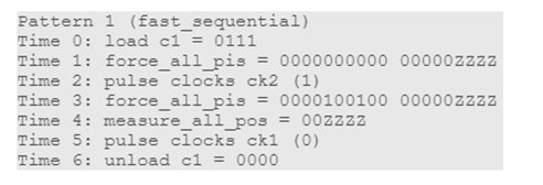
It is a binary format file containing additional parallel strobe required for debugging parallel simulation pattern failures. The data in the PSD file corresponds to the expected strobe (unload scan chain) data coded using two bits model states 0,1 and X. The constructs of the PSD File are shown below Fig. 2:

Fig. 2: Data in the PSD File
The history section of the USF file contains attributes that link the PSD file and the USF pattern file. This information contains STIL Annotation as shown in Fig. 3 below:

Figure 3 Attribute Link between PSD File and USF pattern file
- PSDF - Identifies the PSD file name and location.
- PSDS - Identifies the unique signature (composed of a date and specific ID number) of the PSD file corresponding to the USF file.
- PSDA - Identifies the number of partitions when more than one PSD file is used.
TestMAX ATPG does not use the STIL Include statement to establish the USF to PSD file link. This means the additional parallel strobe data does not need to use the STIL syntax, which could overload the USF file with large amounts of test information.
Steps to create psd file using testmax atpg
There are two ways for creating the PSD File. They are mentioned below:
1- PSD generation using run_simulation command
In this method, you use the -parallel_strobe_file option with the run_simulation command. The following example shows how we can create a PSD file using run_simulation command:
TEST-T> set_atpg -noparallel_strobe_data_file
TEST-T> set_patterns -external usf.stil -delete
TEST-T> run_simulation -parallel_strobe_data_file file.psd -replace
TEST-T> write_patterns usf_resim.stil -format stil -replace -external
TEST-T> write_testbench -input usf_resim.stil -output usf_resim -replace -parameter { -log mxtb_resim.log -verbose -config my_config }
The write_testbench command in the previous example references a configuration file called my_config. This file contains the following command:
set cfg_parallel_stil_report_cell_name 1
2- PSD generation using run_atpg commands
TEST-T> set_atpg -parallel_strobe_data_file psd_file -replace_parallel_strobe_data_file
TEST-T> report_settings atpg
TEST-T> run_atpg
TEST-T> write_patterns out.stil -format stil
TEST-T> write_testbench -input out.stil -output usf_resim -replace -parameter { -log mxtb_resim.log -verbose -config my_config }
The write_testbench command in the previous example references a configuration file called my_config. This file contains the following command:
set cfg_parallel_stil_report_cell_name 1
Practical examples
Example 1 : Messages with no PSD and no Configuration File

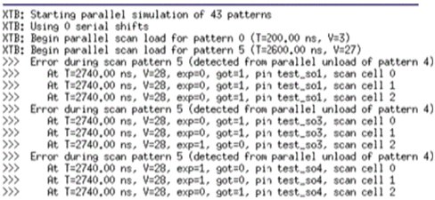
Fig. 4: Error message without PSD and Configuration File
When a parallel compare fails, the bit number listed is the bit in the chain relative to the scan chain output port and the numbering scheme starts from zero. So, bit 0 is the bit that is connected directly to the scan output port, bit 1 is the bit one shift clock away from the scan output, and so forth. So the scan cell bit position can also be thought of as the number of shifts required to move the scan cell data to the scan output. However, this report does not provide the root cause of pattern failure and we still need to backtrace to find the root cause starting from the failing scan cell bit.
Example 2 : Messages with PSD and no Configuration File

Fig. 5 Error message with PSD and no configuration file
As shown in the Fig. 5 we are enabling the enhanced debug mode using a conditional parallel strobe. The tool searches for the corresponding parallel strobe failures and displays the message as shown above providing the exact failing cell location. We have the chain number and the scan cell number. Using this information, we can use the existing scan cell report of the design and find the hierarchy of the failing cell. Further loading the waveforms of the failing cell at failing time instance, we can find out the root cause of failure and perform necessary action on it.
Example 3 : Messages with PSD as well as Configuration File
In the steps to generate the PSD file, we use the configuration option for maxtb generation that is set cfg_parallel_report_cell_name 1. By enabling the enhanced debug mode and using the configuration file in the testbench we can find the cell name and hierarchy of the failing cell.

Fig. 6 Error message with PSD as well as configuration file
This configuration becomes very important if we do not have a scan cell report and we are performing simulation. Further, by using this hierarchy we can directly load the waveforms of the cell and find the root cause in it and take necessary actions to remove the failure.
Conclusion
An efficient method that can reduce the time to debug parallel simulation pattern mismatches was discussed using the Parallel Strobe Data Flow. Adding Design for Testability with the advanced technology nodes increased size, and complex designs it has become a time consuming process, and if the ATPG fail the pattern simulation than it can reduce the time to market. Parallel Data Strobing helps to reduce the tedious efforts of debugging thus proving to be an efficient approach to debug to parallel simulation pattern mismatches. For more information please contact us today.
Authors
 | Saumil Modi is working as an ASIC DFT (Design for testability) Technical Lead at eInfochips (An Arrow Company), Ahmedabad, India. He has more than 8 years of experience in ASIC DFT. He has experience of working on various technology nodes, from 28nm to 7nm, handling different DFX tasks, and manages a team of engineers. |
 | Parth Kadiya is working as an ASIC DFT Engineer at eInfochips, an Arrow company. He has more than 1.5 years of experience in ASIC DFT. He has worked on various technology nodes, like 40nm, 28nm, and 7nm, handling different DFT tasks. |
