Industry Articles
Next Gen Scan Compression Technique to overcome Test challenges at Lower Technology Nodes (Part - I)-October 26, 2020 |
By Sunil Bhatt, Chintan Panchal, Sarthak Tomar (eInfochips, an Arrow company)
Abstract:
We live in an era where the demand for portable and wearable devices have been increasing multifold.
Products based on applications like IoT (Internet of Things), Artificial Intelligence, Virtual reality & Machine Learning are evolving day by day. Smart devices for industrial and home applications Aerospace & Medical applications which are very time critical, Data servers & centers which processes a huge amount of data with lots of calculations & running complex algorithms. All such applications lead to an increase in the CHIP hardware. An increase in the CHIP hardware introduces lots of test challenges at advanced (lower technology nodes).
In today’s scenario, we have designs with more than hundreds of core in an system-on-chip (ASIC/FPGA). As technology is continuously shrinking from 60 nm to 16nm, 7nm & now we are into the DFT implementation at 5 & 3nm lower technology nodes, the number of transistors increases in several million, features in the design is very nearer to each other & it has to address various testability issues like Test Time, Test Data, Pin Count, Test low Power, etc. If these issues are not properly addressed then it will lead to an increase in the test cost &Test area. Sometimes it cannot meet Time to market & the chip might fail on silicon as well.
Introduction:
Multiple conventional Scan compression approaches are available to reduce the test time & test data volume for years & had addressed test solutions at higher technology nodes. Nonetheless, they have certain limitations to address key challenges particularly at lower technology nodes with multimillion flop count design. To address test challenges for the next generation designs, EDA tool vendor, Synopsys has come up with novel compression techniques called ‘Streaming Compression’. In part - | of this paper, we will discuss various features and its comparative analysis with standard compression techniques.
When the design size is with multimillion flop count & design complexities are increasing, Streaming compression offers significant features like reduction in test time & test data volume with optimization in pin count. It is best suited for hierarchical flow as well.
Streaming compression – Architecture
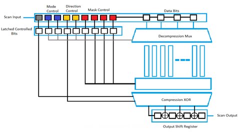
Figure [1] shows that the streaming compression architecture technique supports for single-input, single-output port. The architecture uses shift-registers to scan in and scan out the data at input – Decompression & output – Compression side. The features of the architecture can be divided into the following parts:
- Input Shift Register and Decompression MUX
- Output XOR Compression Tree and Shift Register

Figure [1]: Streaming Compression Architecture from Synopsys
Input (Decompressor):
The input data enters through the scan-in port and goes directly to the input shift register. Here, the input shift register plays two different roles, as it has control registers and data registers:
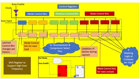
(i) The first group of registers is the control registers. It consists of Mode Control, Direction control & Mask control (Mask Selection) bits. These are all latched to the start of the ATPG cycle for each pattern. The latching function happens when scan enable (SE) shifts from shift to capture. For every pattern, the control registers made up of latches, store the bits. The mapping of the bits from the shift register to the scan chain remains constant for a particular pattern. These control bits are responsible for mapping the data into the decompression logic, which feeds to the internal scan chains, and, for controlling the X-masking logic. The number of control registers present is variable, depending on the design.

Figure [2]: Control Registers Structure & Latching Function
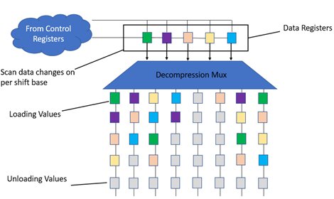
(ii) The second group of internal shift registers is the data registers. Like control registers, the number of data registers present is also variable. The values of data registers are inputs to the Decompression mux logic. Scan data changes per shift basis.
The first bit in the data register enters the codec – Phase shifter (Decompressor) & passes onto the core to the various core chain, according to the latched codec mode. At the same time, the core is unloaded into the MISR & values begin to stream out of the CODEC.

Figure [3]: Loading & Unloading functionality
When the next bit in the data register comes in, the first bit moves onto other scan chains. More unload bits crunch down into the MISR signature. This continues until the entire pattern is complete.
Once the load-unload is completed, data left in the control register (tail) becomes the next patterns control & mask bits. These bits get latched when scan enable (SE) is transitioned. Capture cycle happens next, next pattern can be loaded while the previous one is unloaded (Mode control bits are used for next load while Mask control bits are used for current unload) & these cycles repeat.
Output (Compressor):
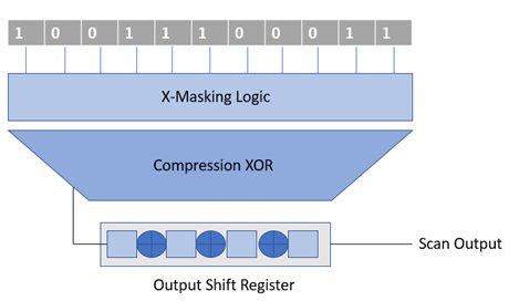
The output of the scan chain is read by the compression logic, made up of XOR gates. The XOR gates are a multilevel network, which simplifies the volume of data coming from the scan chains. These simplified bits get fed into the output shift register. During the capture phase, these registers are reset by the scan-enable signal. The XOR Gates between these registers combine the values coming from the compressor logic and the registers, which is the scan-out value.
One can also use this architecture for multiple scans in and scan out ports, which divides the input and output shift registers into smaller independent groups. In other words, using more scan input-output ports, we get shift registers of shorter length.

Figure [4]: Compressor with O/P shift register
Comparison of streaming compression with Standard Compression
| Streaming Compression | Standard Compression |
|
|
|
|
|
|
|
|
| CODEC is Sequential in nature
|
|
|
|
|
|
|
|
|
|
|
|
| Flows Supported:
| Flows Supported:
|
|
|
|
|
Conclusion:
Architectural features of streaming compression & its comparison with standard compression show that it reduces the test time, test cost & test quality to a great extent. Moreover, it greatly simplifies the task of top level DFT integration & simplifies DFT implementation makes it most suitable to operate at lower technology nodes.
References:
1] White Paper “DFTMAX Ultra”, New Technology to address Key Test Challenges, https://www.synopsys.com/content/dam/synopsys/implementation&signoff/white-papers/dftmax-ultra-wp.pdf
2] https://solvnetplus.synopsys.com/s/article/TestMAX-DFT-User-Guide-version-Q-2019-12
About Authors:
Sunil Bhatt
Sunil Bhatt is working as Senior DFT Engineer in the DFT BU, ASIC division, at eInfochips, an Arrow company. He has more than 3.5 years of experience in Design for Testing, which includes working on 40nm, 28nm, and 7nm & 5 nm technology nodes as a part of SoC projects with different clients. He is handling block-level and top-level DFT activities.
Chintan Panchal
Chintan Panchal is working as a Delivery Manager in the ASIC division at eInfochips, an Arrow company. He has more than 19 years of experience in ASIC DFT. Over the years, he has worked on various technology nodes, from 180nm to 7nm, handling different DFT tasks, and managing a team of engineers
Sarthak Tomar
Sarthak Tomar is working as DFT Engineer in the DFT BU, ASIC division, at eInfochips, an Arrow company. He has more than 1.5 years of experience in Design for Testing. He is handling block-level and top-level DFT activities.
