by Alan Page
Denali Software, UK
Introduction
This paper describes some of the challenges facing designers in implementing the interfaces between ASICs and today’s high performance memory devices. Specifically it addresses the requirements that a memory controller has to meet when being coupled to Double Data Rate SDRAM devices and how designers can achieve these requirements.
Double Data Rate – what is the attraction?
Today, designers are moving increasingly towards the use of Double Data Rate (DDR) Dynamic RAMs for high performance memory orientated designs. Given the increase in complexity of design associated with the move to DDR, this leads to the question, why do it? What is the advantage of transferring data on both edges of the clock as opposed to one?
In the current market for electronic products customers are having ever higher expectations of product performance. The effect of this in the memory market is that designers are demanding more bandwidth from a given device, yet technologies and hence clock rates broadly stay the same. One solution to this problems is to get more data through the available pins on a memory device for a given clock rate. Double Data Rate achieves this by transferring twice as much data through each pin, by the simple expedient of sending two words of data for each clock cycle, as opposed to the traditional one. This implies that the speed of data transfer inside a DDR device is double that of a conventional SDRAM. In fact it is not the case (impossible due to the sharing of similar technologies) and the speed-up is accounted for by using two internal data busses (or one of double width). This has some impact on latency and recovery times which need to be considered when using DDR devices.
Transferring data on both edges of the clock brings new technical challenges that are exacerbated by the high clock rates now available. A complete new clocking scheme is needed, together with a reduction in delay between memory and controller, and revised drivers to deal with signal integrity issues. In addition to this system considerations have to be taken into account in order to fully benefit from the new-found bandwidth available using Double Data Rate techniques. These issues are discussed below, with some ideas about how to circumvent them.
Clock Schemes for DDR designs
DDR transfers data on both edges of the clock. Potentially this sounds simple, data just changes on both positive and negative edges of the system clock. Unfortunately this is not the full story for DDR, as separate clocking schemes are used for both read and write data requiring a clock recovery circuit in both the memory and the controller.
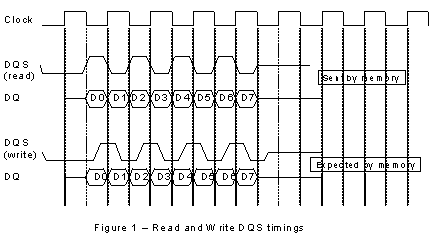
The conventional system clock (as for single data rate DRAMs) is replaced by a differential clock signal (for better noise immunity and edge detection) while for data transfers by a new signal is introduced called DQS. This signal is a bi-directional data strobe that is used for both read and write operations, however the handling of timing is slightly different in each case, with data and strobe edge aligned for read and centre aligned for write (see Figure 1). One DQS signal is associated with a number of data bits, usually 8 (but can also be 4 or 32), and the idea is that the DQS and corresponding data lines experience a similar environment (capacitive loading, routing etc.) which allows the timing skew between them to be minimised and hence a higher data rate to be achieved. As the same strobe is used for both read and write operations (and is controlled by the memory device or controller respectively) a protocol for the usage of the DQS has to be established. This protocol is described below.

Read Cycle
During a read cycle, on the reception of a read command, the memory will take the DQS from a high-impedance state, to a logic low level. This transition nominally occurs one system clock cycle before the transmission of the first bit of data and the low period is known as the DQS preamble. On the rising edge of the DQS the first data bit is transmitted, edge aligned with the DQS. The second bit is transmitted edge aligned with the falling edge and so on until the burst length (number of sequentially transmitted bits) of data is complete after which the DQS returns to a high impedance state. The time between the last negative clock edge and the tri-state condition is known as the DQS postamble. It is not obligatory for DQS to return to the tri-state condition, as one burst of data can follow another and hence a continuous stream of data is possible, with no breaks in between (with some constraints due to row and column accesses).
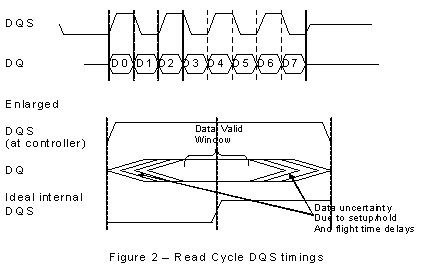
This edge alignment of data and DQS presents a problem when the data arrives at the memory controller. Although nominally edge aligned, there may be positive or negative skew with respect to the DQS and in any case the data ideally needs to be sampled in the middle of it’s data valid window (See Figure 2). The techniques to achieve an ideal DQS/data alignment are various, ranging from using a board based propagation delay, via quarter and half cycle clock delay to sophisticated Delay Locked Loop (DLL techniques), which align data and DQS to within one hundredth of a clock cycle.
The choice a designer makes is dependent on the system performance but the available timing slack can be quite small. Taking a clock period of 10ns, equivalent to a relatively slow 100MHz system clock. The available half cycle time is nominally 5ns, however setup and hold times narrow this window, typically by around 750ps each (accounting for jitter, described later), leading to a data valid window of 3.5ns. This sort of window can be accommodated via a simple quarter clock delay element. However, devices are shortly available at clock rates up to 250-300MHz. At these frequencies the data valid window is getting to the region of 1ns, and here more sophisticated techniques are required.
Write Cycle
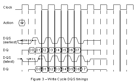
To initiate a write cycle a write command must be issued and then the DQS signal taken to an active low state by the controller. During a write the edge alignment of DQS and data is centred, that is the rising and falling edges of DQS occur in the centre of the data valid window. The actual arrival time of the first positive edge of the DQS can be anything from 0.75 clock cycles to 1.25 clock cycles after the system clock edge corresponding to the write command (see Figure 3). In meeting this requirement the designer has to consider both the output delay of the DQS signal and it’s flight time from controller to memory device, since the arrival time is synchronised with the system clock at the memory rather than at the controller. This can either be done by close attention to board layout and interconnect delays or it is possible in a sophisticated memory controller to use the measured relationship between the read DQS (from the memory) and the system clock to work out the appropriate launch time for the write DQS.


Considerations for bandwidth
The prime reason for adopting DDR devices is to provide increased bandwidth. In practice however, to obtain optimum bandwidth, careful consideration of data type and address space has to be made. DDR devices, like their single data rate predecessors are burst orientated devices. Burst lengths of 2, 4 and 8 are supported and the appropriate value should be chosen based on the likely amount of continuous data. Unlike single data rate devices however there is a write latency associated with DDR. Due to the internal structure of the devices a write command effectively continues after the last byte of data is clocked into the device. This is called the write recovery time.
As with reads, writes can be concatenated together to effectively give a continuous data stream. However, when going from a write command to a read command, both the write postamble and read preamble times contribute to a significant turn round delay. Sequential reads and writes are only possible providing the data is within the same row, moving from one row to another, requires a delay for row closure and opening. Another delay effect is the action of precharging the row on closure to ensure data retention. All of these effects mean that DDR devices are ideally suited for large data transfers in one direction i.e. a long set of reads followed by a long set of writes, rather than random reads and writes.
To a certain extent advantage can be taken of concurrency in dynamic devices. It is possible to take advantage of the banked structure of the memory devices to access data in one bank, while completing operations in a second. This brings into play the idea of bank cycling. This technique requires that reads and writes from different rows are not done sequentially within the same bank, but occur sequentially in different banks. Opening a row for access requires a sequence of actions (selecting row followed by column) which are summed into the CAS latency for the device. DDR devices typically have CAS latencies of between 1.5 and 3 clock cycles. Obviously if the designer has to wait for 2 clock cycles before getting data each time, then the overall throughput of the device will suffer. The workaround is to arrange to access data in sequential banks, which allows the overhead of enabling rows and accomplishing precharging to be done in parallel, thus minimising the overhead. Bank cycling does however impose some restrictions. The bank address lines occupy some space (two bits) in the overall memory map. In order to be able to read sequentially from each bank in turn the data must be arranged such that the addressing requires a sequence through the 4 banks in turn. For predictable systems this is possible, but for less predictable systems where data is highly random (such as graphics processing or networking) an alternative may be needed.
An improvement in throughput can be achieved by careful design of the memory controller. If a queuing system is implemented then the controller can use look-ahead techniques to see which addresses need to be accessed and minimise any unnecessary row closures. Alternatively the use of specialised double data rate devices may be more appropriate. These are described below.
Specialised DDR devices
DDR memories are generally defined according to a JEDEC specification JESD79, which sets out the modes of operation of these types of devices. Recently, as designers have tried to find ways around the latency of DDR devices, some specialised alternatives have evolved. There are two main derivatives of double data rate devices, these being Fast Cycle RAM and Reduced Latency DRAM. These alternative devices offer some structural changes, which help to reduce the overall latency in the device and in some cases reduce power consumption too.
RLDRAM offers an 8 bank structure, with hidden precharge times, whereas FCRAM retains the 4 bank architecture, but uses hidden precharge to improve access time and partial word line activation to reduce power consumption. In general these techniques decrease latency and improve access times for random accesses, however there are some constraints that may act against the improvements. For instance FCRAM cannot interrupt a command, which means memory accesses must be word aligned, or a read-modify-write technique used if byte aligned data access is needed. These types of restrictions must be studied carefully to ensure that potential performance improvements can indeed be realised.
DDR Specific Design Considerations
There are a few differences (apart from the clocking schemes) that pose extra design requirements for a DDR memory controller when compared with traditional SDRAM.
Device Initialisation
DDR devices have a complex initialisation scheme which must be followed in the memory is to be successfully brought to a known state. The full initialisation process is beyond the scope of this paper, however some basic rules will be discussed
Firstly, the power supplies to the device must be established in the correct order. First the main power supply VDD (which can be 3.3 or 2.5 volts dependent on device) must be applied. Secondly the data bus power supply VDDQ (2.5 volts) must be applied, and then last of all VREF the reference voltage for the SSTL2 pads, which should be applied simultaneously as the system VTT termination voltage. VREF is defined as half the VDDQ of the transmitting device and has a quite stringent noise immunity specification, with less than 50 mV of noise being allowed on the input.
During the establishing of these voltages the CKE (clock enable) pin should be held low to ensure that all DQ and DQS signals are high-impedance. Once all voltages are stable a pause of 200 usec is necessary before applying any commands.
The first command that should be applied is a Precharge all, followed by setting of the internal register of the device. The internal mode register settings define the operation of the device, from CAS latency to burst length and burst mode to enabling and disabling the internal DLL..
Data Masking
Data masking is possible for DDR in a similar way to SDRAM. However data masking is only possible during write, not read and the DM inputs are sampled on both edges of the DQS data strobe in a similar way to the active data pins. DM inputs are loaded internally to the memory device such that although unidirectional, they appear as a similar load to the data bus, enabling synchronising of timing to be simplified.
Refresh operation
A DDR device needs to be refreshed periodically to prevent data loss. Refreshing is done by rows and the total maximum refresh interval (e.g. 64msec) is divided dependent on the memory architecture into an average interval for each refresh, known as TREF. This typically would be around 15usec (64msec/4096). In theory if a user can guarantee to access every row in a device at least once each 64msec then all data will be refreshed and explicit refresh cycles for individual rows would not be necessary. In practice however, the period access to rows cannot be guaranteed. Furthermore some memory devices use the refresh time to resynchronise their internal DLL and therefore explicit refresh cycles are required. In order to make a memory controller flexible to handle different DDRs and “futureproof†then an explicit refresh counter needs to be implemented.
IO Drivers
DDR devices use high performance SSTL-2 IO pads, at a minimum for the clock, data, DQS, DM and CKE pins. These pads use a differential signalling mechanism, with threshold voltages above and below the reference voltage, which is mid-rail. A full description of the SSTL-2 standard is available in JEDEC specification JESD8-9.
A typical termination network is a 25 ohm resistor between driver and load, with a parallel 50 ohm resistor connected to the threshold voltage VTT. This network can be varied according to driver class of which there are three.
The above network applies to a class 1 driver, which must be able to drive 7.6mA. The paralleled 50 ohm resistor can be changed to a 25 ohm value for a class 2 driver (15.2mA).
Some device manufacturers support a lower level drive capability which is designed for matched impedance networks, that employs a 5mA drive capability.
It is an option to use LVTTL pads for the command lines, similar to all pins on a SDRAM device.
Summary
The move to Double Data Rate SDRAM is not a trivial exercise. However with careful memory controller design, considering all the specialised requirements, a high performance, high bandwidth system can be realised in a cost effective way. Some of the potential pitfalls in the design process are considered above and there is nothing in the specification for DDR that should discourage the experienced memory controller designer. However if it is a first time memory controller design and/or a first time for DDR, then there is a potential for errors to cause project milestones to be missed and in this case the use of pre-configured and tested IP for the memory controller may be a wise, if conservative decision. Denali provides a product called Databahn, which is a fully configurable piece of IP, which addresses all of the issues described above. Since there are a wide variety of DDR devices available, the IP has to be configurable to support all of them, yet able to perform at the high frequencies necessary to support the bandwidths required. This is done by a combination of a synthesisable RTL description, together with technology specific netlists, both of which are tailored to a project’s individual requirements.
