by Emre Tuncer and Wolfgang Helfricht
Monterey Design Systems, Inc.
Sunnyvale California, USA
Abstract:
Deep sub-micron effects complicate design closure for very large designs. Top-down hierarchical design methodology combined with physical prototyping increases design productivity and restores schedule predictability. In this paper a top-down hierarchical flow will be discussed and use of physical prototyping to predict the performance and physical characteristics of the final physical implementation will be explained.
TOP-DOWN SOC DESIGN METHODOLOGY
System-on-Chip (SoC) designs have become one of the main drivers of the semiconductor technology in recent years. Multi-million gate designs with multiple third party intellectual property (IP) cores are commonplace. SoC designers employ IP reuse to improve design productivity. Previous designs done in-house or third party designs can be used as IP in the current design. While employing IP cuts development costs and time, integration complexity increases.
This is one of the main reasons why SoC designs are implemented with hierarchical top-down design flows. These flows help to manage the different and conflicting requirements of increasing design size, deep-sub micron effects (DSM) and the necessity for shorter and predictable implementation times. Hierarchical methodologies allow multiple teams to work on different parts of the design concurrently and independently. This “divide and conquer†approach reduces the complexity of the design problem for each design team and reduces the time to market. For the SoC designs, which are built from independent function blocks, these capabilities are key advantages as the final implementation of complex chips can be a lengthy process and parallelization can save valuable time. Hierarchical design styles also allow for much faster and easier late ECO’s. Functional changes may be localized to a single block leaving the remainder of the design unaffected. This localization results in faster, easier ECO’s.
Another reason for hierarchy is to overcome the capacity limitations of design tools. Hierarchical design flows are scalable to handle designs containing upwards of 100 million gates.
In addition to the complexities that are a result of large design size, deep sub-micron effects add to integration complexities and cause late stage surprises and large loops during the design cycle.

In deep sub-micron technologies, wires, power, routability and manufacturability have to be considered early in the design cycle. Physical prototyping provides early feedback in terms of design closure and helps validate the correctness of design decisions. Physical prototyping should accurately predict the characteristics of the final physical implementation. This can be accomplished by performing cell placement and global routing at an appropriate level of granularity needed to ensure that the prototype correlates to the final implementation within a specified tolerance.
Traditional, top-down SoC designs rely on the assumption that the budgeting performed at the chip-level need not be revised after the blocks are implemented. However, unless very conservative budgets are used, it is impossible to predict upfront whether the final block implementations will meet all constraints. Also, it is difficult to adjust the budgeting if we cannot capture the physical properties (e.g., driver strength, parasitics, current drain, etc) that are observed at the block and chip boundaries. A top-down hierarchical design methodology should therefore be combined with physical prototyping to enhance design productivity and restore schedule predictability . In this paper, a top-down hierarchical block-based flow will be discussed and use of physical prototyping to predict the performance and physical characteristics of the final physical implementation will be explained.
HIERARCHICAL SOC DESIGN FLOW
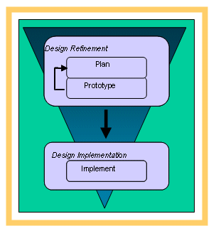
The components of a predictable top-down hierarchical flow are design planning, physical prototyping, and implementation. At the design planning stage, chip topography, area, number of chip level partitions and timing budgets are determined. During physical prototyping, the design planning results are validated for each block and for the top-level. If necessary, corrective action is taken by going back to design planning and progressively refining the design. Once physical prototyping results are satisfactory, implementation can commence concurrently for each block and for the top-level, with the assurance that design-planning decisions are correct and implementation will be completed without any late surprises. Top-down planning and bottom-up prototyping is the most predictable way to achieve closure on large SoC designs.
Design planning constitutes an important portion of the top-down hierarchical design flow. The SoC designer evaluates tradeoffs with respect to timing, area, and power during design planning. At this stage, various IP cores from different vendors are integrated into the design along with custom logic. The IP may be provided as RTL code, gate level netlists, or fully implemented hard macros. Decisions regarding choices of different implementations of the same IP, chip and block aspect ratio, budgeting of top-level constraints, standard cell utilization, and other design aspects are made during design planning .
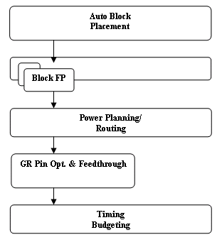
Design planning functions include partitioning of the design, block placement and shaping, hard macro placement, pin assignment and optimization, top level route planning, top level repeater insertion, block budget generation, and power routing. All of these functions are closely linked to the underlying physics of DSM technology. For example, top-level repeater insertion cannot be done properly without considering signal integrity and pins cannot be assigned without considering antenna rules.

Design planning can start upon availability of the initial top-level netlist, even if the modules have no internal definition or structure. At this stage missing modules are represented as black boxes. The areas of black boxes are user defined and quick timing models are generated for setup/hold arcs and clock-to-output delays. Area estimates for modules that have already been synthesized will be determined by the gate count and user defined utilization.
Once the design is read in, and block sizes are determined, an initial floorplan is created by automatically placing all blocks, shaping the soft blocks, and packing the blocks together based on global routing information. Using the block placement results, adjacent blocks may be clustered together, or very large blocks may be divided into smaller blocks. Modifications of the physical hierarchy at this stage may be made to take full advantage of the physical implementation tools, and to minimize the number of top-level blocks.
The block placer must also be able to automatically perform such operations as determine the best aspect ratios for soft blocks and choose the best among different equivalent implementations of hard blocs. A combination of the block placer with a memory or macro generator leads to optimized SoC blocks as the design planner finds a global optimum between the different possible implementations and the chip plan. After initial block placement, top-down pin assignment is performed; top-level connectivity and timing drive the placement of the pins on the blocks. For RTL or black box modules, pin assignment will help to create block-level constraints. Once the physical locations of pins are known, top-level net lengths can be estimated.
For each block, an internal design plan is created. Macro placement is driven by both top-down pin assignments that were done in the previous step and internal metrics such as connectivity, timing and area. Once the internal planning for all blocks has been completed, power route planning is done. Most recent technologies require a mesh structure. The power routing grid and block placement grid should be carefully set to prevent connectivity problems that may arise due to misalignment of a block with respect to power grid.
After power routing, pin assignments are refined using global routing results. The global router can identify narrow or wide channels and move blocks around to open up congested channels and constrict sparse ones. This enables optimum pin placement for routability during the implementation stage.
Another complexity facing SoC designers during design planning is top-level route planning. Nets between critical blocks must be as short as possible and should often be routed over other blocks. These over-the-block nets should be pushed down into the blocks automatically. This requires that a number of operations take place. Pins must be assigned to the block to accommodate this new feedthrough net. Both the top-level and internal block-level netlists must be altered to add connectivity to the feedthrough net. Top-level timing budgets must be adjusted and internal block-level budgets must be generated to account for global timing closure and signal integrity. The use of routing over blocks may even include reserving special routing channels and empty placement areas for repeaters. Altering blocks in this way conflicts with the goal of having separated, or even re-usable SoC blocks, so it depends on the overall project goals to what extent such techniques are used. If turn-around time (TAT) or re-use are the primary goals, such techniques should used very carefully. If smallest die size or best design performance are primary goals, then the use of feedthroughs may be essential to achieving the goals.
During timing budgeting, delay of top-level nets should be calculated with the assumption that buffers will be added to long or high fan-out nets as needed. Block budgets will be used as constraints to drive synthesis, prototyping, and implementation of the blocks.
In practice, planning may begin before all of the blocks are fully implemented, so rough estimates are initially used instead. As the blocks progressively gain definition, it is necessary to relay the new block information back up to the chip-level, where it is incrementally updated and the appropriate adjustments are made. This may trigger changes at the chip level that must be pushed back down to the block level. This leads to a top-down budgeting, bottom-up prototyping flow, which is more predictable and better suited to handle variances between block-level constraints and actual implementation.

Although it may appear that there is a conflict between early design planning using black-box models or RTL and netlist-based design planning this is not the case; these activities actually complement each other. Early top-down design planning is an important step to drive RTL synthesis and to generate a gate-level netlist that is used to further refine the design plan.
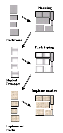
A characteristic of the continuous planning and optimization process is the use of different types of models that are optimized for the different operations in the process. This is illustrated in the figure above. Simple block models are used for design planning and budgeting. The physical prototypes of the blocks are built based upon the budgets from the design plan. The physical prototypes provide valuable physical information about the final implementation of the blocks. They will be described in the next chapter. The physical prototypes are then used to replace the black boxes and RTL modules at the top level, so that we can refine the chip-level constraints. When the final budgeting is resolved, we return to the blocks and resume their implementation, and then we finish with the top-level chip assembly.
Also, different types of models can be mixed at the top level since it is likely that all prototypes will not be completed at exactly the same time. This enables early verification and adjustment of the chip-level constraints using a combination of black boxes or RTL for some blocks, accurate prototypes for others, and even completed physical layouts for some of the blocks.
Physical prototyping is an important stage of the hierarchical design flow as it provides more details about the block implementation to the SoC designer. It bridges the gap between logical and physical design by adding physical reality to the abstract view of the design planning process. During physical prototyping, logic optimization and global placement are concurrently applied. At this stage, design-planning results are validated for each block and for the top-level, and all conflicts are resolved. The prototypes uncover the problems; the corrective action is taken in the design planning stage. Incomplete timing constraints can be discovered and addressed with the availability of accurate physical information.
Physical prototyping is inseparably connected with the physical synthesis process that addresses many DSM issues by combining elements of logic synthesis and physical implementation together into a single stage . Physical synthesis, as most people use it today, starts with a gate-level netlist and performs logic optimization, placement and global routing, to produce a placed design that meets timing requirements. Physical synthesis may employ numerous techniques to optimize the logical structure of the chip including: gate sizing, buffering, pin swapping, gate cloning, useful skew, re-synthesis and technology re-mapping, redundancy-based optimization, and area and power recovery.
This is a significant improvement over pure logic synthesis because the logic optimization is performed and evaluated based on cell placement that is indicative of the final placement.
It is significant to note that it no longer makes sense for RTL-to-gate synthesis tools to perform sophisticated gate-level optimization. Without accurate physical information, logic synthesis tools cannot make good decisions about cell sizing or buffering. Physical synthesis is much better suited for these tasks. Today, the role of RTL-to-gate logic synthesis has been reduced to simply producing a structural gate-level netlist as quickly as possible, and then pass it along to physical synthesis without attempting to optimize the sizing or buffering aspects. This has consequences for IP cores, which are delivered as soft macros from the IP vendor to the user or implementer. The IP provider delivers either the final hard macro or an RTL/netlist and implementation constraints to allow the optimization of the IP during the implementation of the SoC chip.
All the information generated during the physical prototyping of blocks plays a key role in feeding back more accurate information to the design planning stage for refinement of top-level design parameters.
The physical prototype consists of a coarse placement and optimized netlist. Power routing, clock tree buffers, high fan-out net buffering must be included in the physical prototype. Without any of these items, physical prototype will not correlate to implementation and will not give useful results.
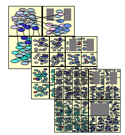
To create the physical prototype, a hierarchical tree of cell-clusters is built from the original netlist before the placement starts. While building the tree, functional hierarchy and connectivity are considered. Then, the block area is divided into placement bins, and the cell-clusters are assigned to bins among hard macros. The congestion is modeled using wires crossing bin boundaries. During the early stages, the bins are very coarse and it is not useful to measure timing since most of the wire capacitance is due to intra-bin nets and can only be statistically estimated. As placement progresses, the block area is further divided into smaller bins, and placement is refined, to improve both congestion and wirelength. The bins continue to get progressively smaller in size until at some point, the global wires can be accurately estimated, and intra-bin wire uncertainty is negligible . Physical synthesis can now start and the netlist is transformed to meet timing constraints. The placement is not yet finalized, hence, the impact of netlist optimization operations such as long net buffering, sizing, fan-out optimization, technology re-mapping, etc., can be easily absorbed. The picture below shows this design process.

Similarly, clock tree synthesis can be done at the physical prototyping stage assuming the leaf instances are placed at the center of the bins. Congestion and utilization estimates are more accurate with the inclusion of clock tree buffers.
Physical prototypes are used to validate timing budgets, area budgets, IR drop, congestion, and pin locations. The feedback from physical prototyping back to design planning contains accurate timing abstractions (for refining budgeting at top-level), power models (for top-level IR-Drop analysis), and congestion hot spots, which need to be addressed by relocating pins or hard macro placement.
The top-level physical prototype will provide feedback on top-level timing closure, routing congestion, and required channel area for buffering both clock and signal nets.
As the design becomes more and more defined, the loops between the design planning stage and prototyping will converge. Once all blocks and the top-level are defined, the SoC designer is ready for implementation.
Sign-off is the delineation between the design refinement process described above and the final implementation. It has changed over time to accommodate the new requirements associated with DSM process technologies. In the past, a netlist hand-off was sufficient and provided a reliable interface between logical and physical design. As we have seen in the previous chapter, a netlist generated by RTL synthesis is no longer the final netlist. Instead a prototype containing an optimized netlist and a coarse or even final placement are used to sign-off the design prior to final implementation.
Implementation completes the process by transforming the prototype into a final physical layout. Implementation operations include detailed logic optimization, placement, and routing. Throughout the process, the design is being continuously monitored for timing, power, clock skew and delay, IR drop, and signal integrity. Once the blocks are finished, top-level assembly is done. Since the block-level implementations were driven by top-down constraints, top-level surprises are eliminated.
As mentioned above the starting point for final implementation can be a prototype with a course placement, in this case the final implementation proceeds using the same technology as was used to generate the physical prototype with progressively smaller and smaller bins. At each bin level, congestion, wirelength, and timing optimizations are incrementally run. If the starting point for implementation is a final placement, then the implementation stage proceeds with the routing and adjusts the placement as needed.
Accurate abstractions of completed blocks are needed to perform top-level assembly and sign-off the design for tapeout. Timing models should include interface parasitics, account for signal integrity, and should be able to consider timing exceptions on nets that cross block boundaries. Physical models should correctly represent embedded wide wires, via cuts near the boundaries of blocks, antenna models, and electromigration effects.
Top-level clock tree synthesis plays an important role in reducing hold violations. At the top-level, clock trees are synthesized such that skew to each block input is adjusted to account for the insertion delay inside the block. The top-level setup and hold violations can be identified and fixed with block timing abstracts generated using propagated clocks. The skew to each register connected to a block-level clock pin will be included in the timing abstract if a propagated clock is used during abstract generation. At the top-level, setup and hold violations between clocks can be identified and addressed.
CONCLUSION
IP reuse in SoCs bridges the design gap by improving productivity but at the same time, DSM effects complicate integration. The only way to restore predictability to design cycle is through top-down design planning, combined with fast and accurate physical prototyping. Block-based design planning addresses increased complexity; while physical prototyping restores predictability and improves turnaround time by taking into account uncertainties due to wires and other DSM effects.
1- François Remond, The Work Flow of a Block-Based Design Team, Integrated System Design, December 2000. http://www.eedesign.com/editorial/2000/designtools0012.html
2- A. B. Kahng. Classical Floorplanning Harmful?: Proc. ACM Intl. Symp. On Physical Design, 207-213, April, 2000.
3- O. Coudert, Rapid High Capacity Prototyping and Physical Synthesis: In Proceedings of the SAME 2002, October, 2002.
4- Karypis, G., Aggarwal, R., Kumar, V., and Shekhar, S. Multilevel hypergraph partitioning : Application in VLSI domain. In Proceedings of the Design Automation Conference, June 1997, 526-239.
5- Padmini Gopalakrishnan, Altan Odabasioglu, Lawrence T. Pileggi, Salil Raje: Overcoming wireload model uncertainty during physical design. ISPD 2001: 182-189
