By Tony Pialis, Clint Walker (Alphawave IP)
Abstract
This paper covers:
- Brief introduction to high-speed, interface basics, as well as the industry motivations driving demand for 200 Gigabits per second (Gbps) connectivity.
- Review of the challenges faced with scaling rates to 200 Gbps and the different modulation schemes needed to accomplish the feat.
- Various approaches used for implementing receivers at 200 Gbps, as well as error correction and coding approaches for improving the associated bit error rates.
- Review of some real life 200 Gbps channels and simulation results.
- Conclusions, findings, and predictions for 200 Gbps serial links.
Introduction to High-Speed Interface Basics
Figure 1 shows the basic blocks of any connectivity interface.
Figure 1: Plot of a Communication System
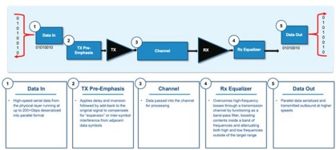
In electronic systems, connectivity functionality is ubiquitous and used wherever a chip must be connected to another chip. Connection length can range from distances spanning thousands of miles, which are traditionally addressed by high-speed optical networks, to short chip-to-chip links used to connect chips to each other. As every chip functions internally using electrical signaling, the electrical connectivity interface is an essential functional block of semiconductor design.
All computer chips use digital data. They come in byte and words. One byte consists of up to 8-bits of data, while a word consists of 1 to 16 bytes. A Serializer/Deserializer (SerDes) is used in integrated circuits as an interface to other chips by converting parallel streams of data, which are used within integrated circuits, to serial streams, which are used in longer-distance transmission outside and between chips, and vice versa. In general, serial transmission is more efficient and less complex over longer distances due to timing, synchronization, and footprint advantages, whereas parallel transmission is critical inside chips to achieve throughput and performance. Due to this key difference, every integrated circuit that needs fast and reliable external connectivity requires a SerDes.
A SerDes consists of both a transmitter and a receiver. A transmitter takes parallel data words, serializes them and pre-conditions them for the channel. Pre-conditioning converts the digital words into a real-world analog waveform from which the transmitter drives the signal over the channel. The channel can be a copper cable, optical cable, electronic board, and so on.
Eventually, a receiver accepts the real-world data from the channel. It then conditions it, equalizes it, and resamples it to compensate for the noise and interference introduced by the channel. Ultimately, the receiver converts the real-world signal back to digital 1’s and 0’s, data bytes, and data words.
The Industry Needs 200G Connectivity!
Figure 2: Industry Trends Driving the Adoption of 224Gbps Standards
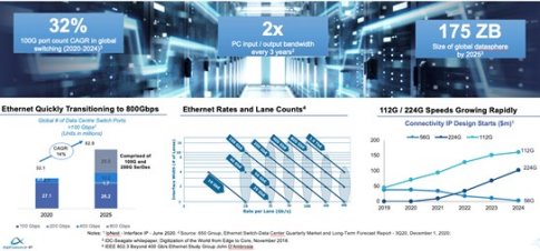
Over the last decade, the proliferation of new technologies, applications, cloud-based services, and internet-connected devices has led to increasing levels of data traffic and congestion, driving the need for greater bandwidth. The global datasphere, or data that is created, captured, copied and consumed is set to grow from 40 zettabytes in 2019 to 175 zettabytes in 2025, representing a Compound Annual Growth Rate (CAGR) of 28 per cent. A significant portion of this data has to be transmitted using wired network infrastructure. The following factors drive this rapid creation and consumption of data, including:
- Proliferation of cloud services and hyperscale data centres. Enterprises are increasingly adopting cloud services to reduce IT costs and scale computing, networking and storage requirements on-demand. Consumers are increasingly relying on cloud services to satisfy bandwidth-intensive needs such as high definition and 4K on-demand video viewing, audio streaming and photo sharing. The global cloud services market is expected to grow from USD $552 billion in 2020 to USD $1 trillion in 2025.1
- Development of advanced wireless technologies, such as 5G. Consumption of data and video-intensive content and applications on mobile devices is driving significant growth in mobile data and video traffic and has led to adoption of advanced wireless communication technologies, such as 5G. By 2023, average mobile speeds of 5G-enabled devices are expected to be 575 megabits per second, or 13 times higher than the average mobile connection today.1 To support cellular speeds of such magnitude, wired connectivity interfaces must match this performance, particularly as wireless signals aggregate in the access layer before being routed to core wired networks.
- Proliferation of “Internet of Things” devices. Significant consumer, enterprise and governmental adoption of internet-connected devices embedded with electronics, software and sensors is anticipated to strain network capacity further and increase demand for bandwidth, while creating significant amounts of data to process. Approximately 29 billion devices and objects are expected to be connected to the internet by 2023, compared to 18 billion in 2018.1
- Growth of artificial intelligence. Proliferation of hyperscale data centres, improvements in hardware and semiconductor technology and maturation of software frameworks has fuelled significant growth in artificial intelligence applications. Compute devices such as microprocessors (“CPUs”), graphics processing units (“GPUs”), field programmable gate arrays (“FPGAs”) and specialised application-specific integrated circuits (“ASICs”) can now be configured to train and apply complex machine learning models and make accurate predictions that were not possible a decade ago. As these models become more multi-layered and complex, they need to be processed on many interconnected computing cores, which puts significant pressure on wired connectivity and interface technologies.
Consequently, to enable all this increase in bandwidth, Ethernet rates are scaling quickly from 100 Gbps links to all the way up to 800 Gbps links. The current leading generation of Ethernet is 400 Gbps Ethernet. However, the next generation of 800 Gbps Ethernet is estimated to have 25 million units shipped in 2025, far exceeding the deployment of 400 Gbps Ethernet. Initially, 800 Gbps links will be comprised of eight lanes of data operating at 100 Gbps. But the vast majority of 800 Gbps deployments will use four lanes running at 200 Gbps. The market is expecting that by 2024 there will be more than 100 design starts integrating 200 Gbps SerDes IPs1.
Challenge of Scaling Symbol Rates to 224 Gbps
Figure 3: Tradeoffs of Scaling PAM4 to 224 Gbps
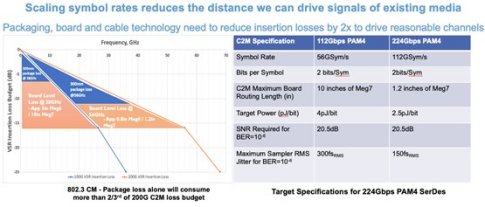
The plot in Figure 3 shows the current 100 Gbps IEEE 802.3ck ‘Chip-to-Module’ specification for optical interfaces. The standard assumes a 30-millimeter package, which has approximately 6.5 dB of loss at 28 GHz. Thus, in a total 16 dB loss budget, approximately one third of the loss is allocated to both transmit and receive packages, which results in approximately 12 dB of loss allocated to board level losses.
At 28 GHz, 12 dB of board level losses results in approximately five inches of reach for Meg6 materials, and approximately 10 inches of reach for newer Meg7 materials. Practically, this means you can drive almost a foot of board in between your large switching SOC and optical module.
By scaling the symbol rate to 200 Gbps using PAM4 modulation, the same 30-millimeter package at the 112GBd symbol rate would now consume approximately 12 dB of loss. That leaves about a third of the loss budget for the board. Assuming the same equalization levels would be applied to the 224G ‘Chip-to-Module’, would result in less than 1-inch of Meg6 material being available between the switch and the optical module. The newer, more costly Meg7 material achieves a full 1.2 inches of distance between the two devices. Obviously, this is a dramatic reduction from the foot long separation that is tolerable at 112 Gbps—down to only one inch at 224 Gbps. Building systems using optics would clearly be unwieldy with these types of routing restrictions.
This is a challenge that must be overcome for the industry to successfully scale designs up to 224 Gbps.
High-Capacity Modulation Schemes
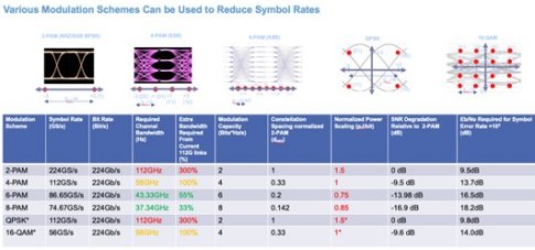
Figure 4: Comparison of Various Modulation Schemes
Given the projected material advancements in package, board substrates and high-speed cables, system designers must also develop schemes for increasing the data throughput of existing channels to enable the continued scaling of data rates.
Reviewing the different types of modulation schemes available, such as PAM and NRZ signaling, NRZ is just one class of PAM signaling (also known as PAM2). If you drive one volt peak-to-peak, regardless of the modulation scheme, the separation between the two constellation points can be electrically classified (logically) as plus three to minus three. So the separation between these two constellation points is 6.
When you look at PAM4, assuming the same maximum swing applies to all signaling schemes, the electrical levels are now - 3 - 1 +1 +3. That is, the separation between any two constellation points is now only two units, which is a reduction of three compared to NRZ.
This reduction in constellation point spacing is why system designers typically state there is 9 dB of degradation in the Signal-to-Noise Ratio (SNR) when implementing PAM4 versus NRZ. It is because for the same maximum launch, the separation between constellation points is reduced by 9 dB, which in turn may make the design 9 dB more sensitive to noise and losses between these two schemes.
When considering higher order modulations, such as PAM8, a 33% increase in bandwidth is required to transmit at 224 Gbps because now systems transmit three bits for every symbol. Therefore, bandwidths relative to current PAM4 systems would only need to increase 33%, whereas PAM4 for systems at 224 Gbps would need to double their required channel bandwidth—which does not look imminent anytime soon.
Similarly, to use NRZ, a three-fold increase is necessary relative to the currently available 112 Gbps systems, which is clearly not feasible.
However, for PAM8, spacing between adjacent constellation points is reduced from two units down to about 0.86, relative to NRZ. This is approximately a 7 dB SNR degradation relative to current PAM4 systems. So PAM8 is a modest 33% increase in channel capacity, but with about a 7 dB further SNR degradation from systems built currently.
In addition to PAM, there is also Quadrature Amplitude Modulation (QAM), where a signal is split up into two orthogonal vectors: in-phase and quadrature. For QAM systems, part of the signal is encoded using the in-phase portion of the signal, while the other part is encoded using the quadrature phase. These signal parts can then be modulated with the carrier and both orthogonal signals can either be carried by the carrier or via time-domain multiplexing to avoid needing a carrier altogether.
The benefit of QAM modulation is that by transmitting the signal onto orthogonal vectors, the SNR degradation is much less when compared to PAM since we can space out the constellation points much further in two dimensions, whereas PAM only spaces them out on a single dimension. However, one of the drawbacks of QAM is that to implement the modulation with either carrier or time division multiplexing, system designers must double the bandwidth relative to PAM. This bandwidth increase is not feasible and makes QAM less desired approach.
Thus, there is no easy modulation choice. Higher orders of PAM require less channel bandwidth, but SNR continues to degrade. In turn, reach is reduced because of SNR limitations, unless system designers can implement new equalization approaches to recover the lost performance.
Advanced DSP Detectors
Traditional FFE/DFE architectures make slicing decisions based on a single data symbol. Maximum Likelihood Sequence Detectors (MLSDs) use Viterbi Detection to make slicing decisions based on a sequence of data symbols. This means MLSDs:
- Minimize errors across a sequence of symbols.
- Use inter-symbol interference to make better decisions.
- Improve SNR by about 1 to 3 dB
Figure 5: MLSD Decision Trellis Example

Use of more advanced DSP approaches such as MLSD helps to improve the SNR. Although transitioning to PAM8 degrades SNR by 7 dB, system designer can offset some of the SNR loss by recovering the signal using more robust approaches like MLSD. These detectors are like a DFE in that you do not amplify a recovered signal which includes the noise.
The concept of MLSD is that an ideal vector is passed through a FIR filter based on both a known channel response and the minimum mean square error between this reconstructed signal. When the signal is passed through a decision trellis, it shows what the ideal signal would have looked like at the output of the FIR filter that is matched to the channel. Finally, the projected signal response from the output of the decision trellis, is compared to the actual signal recovered, to determine the original data transmitted.
The real power of a MLSD is that it does not decide based on a single bit of data. Decisions are made at the outputs of a decision trellis, using a matched channel filter, based on multiple symbols of data to help drive towards a more reliable choice.
Slicing based on a sequence of symbols can improve SNR anywhere between 1 to 3 dB. Therefore, if transitioning to PAM8 reduces SNR by 7dB, a MLSD detector can be employed to add back in up to 3dB of SNR gain. This now leaves only a 4 dB gap remaining to recover through some alternate means.
2m Cabling Silicon Results
As shown in Figure 6, using MLSD delivers a 1.5 order of magnitude improvement in BER.
Figure 6: Measured 112 Gbps 2m Cable Response
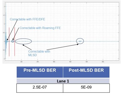
The plot in Figure 6 is an example of how powerful MLSD detectors can be when used in a real-world system. In this plot there is a significant number of reflections that fall within the first 80 symbols of the main pulse. These are typically correctable using FFEs and DFEs. However, there is still a significant amount of energy beyond a hundred symbols. Normally these reflections can not be equalized and are viewed by the receiver as noise and ultimately degrade performance.
However, by using MLSD receivers the impacts of this noise can be minimized since noise is averaged across multiple symbols before a decision is made. In the example above, almost two orders of magnitude BER improvement is achieved using MLSD detectors.
High Performance Error Correction
Concatenated codes can extend performance with only a nominal increase in latency and power. Hence, Forward Error Correction (FEC) is a scheme that has been broadly used in RF read channels, VDSL, and cable modems as a means of making systems more robust while running with a lower SNR.
Figure 7: The SNR Benefits of FEC
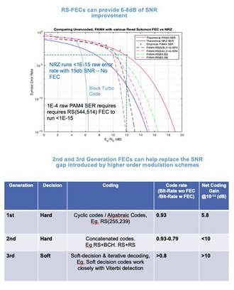
Figure 7 shows a plot of estimated BER versus SNR (EBNO) of a raw PAM signal. The red curve is a plot of symbol error rate versus SNR for PAM4, and the blue curve is the same plot but for NRZ. For the PAM4 signal, at a 1E-15 BER, approximately 19 dB of SNR is required compared to only 15 dB SNR for a NRZ signal. This is the clear advantage offered by NRZ, which allows it to tolerate a lower SNR while still having an equivalent BER.
Referring to Figure 7, assume that the raw SNR for a PAM4 signal is 12 dB with a corresponding BER on the order of about 1E-4. If a Reed-Solomon KR4 FEC is used, that raw BER is lowered to 1E-15. Thus, for the same SNR, FEC produces almost a 12x improvement in error rate.
Some of the drawbacks of FEC, is that it inserts extra information into symbols, reducing the information throughput (this can eat up anywhere between 10 to 20% of data throughput). Second-generation FEC can provide up to 10 dB of code gain, while still higher coding gains are achievable based on ‘soft decision-making’ and iterative decoding FECs, such as block turbo codes.
224 Gbps Modulation Simulation Results
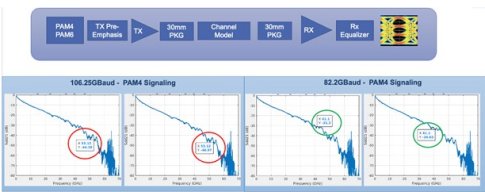
Figure 8 analyzes and compares the performance of PAM4 and PAM6 signaling across two sets of channels. Both sets of channels use representative 30 mm package S-parameter models on both sides of the link, as well as an internally derived transmission line model for the channel. The diagram compares the loss at Nyquist for both PAM4 and PAM6 signaling:
- PAM6 has a lower Nyquist rate, so it only exhibits 31 to 34 dB of loss at Nyquist (41.1 GHz) compared to PAM4, which exhibits 44 to 47 dB of loss at 53.12 GHz.
- This difference in baud rate introduces an additional 12 dB of loss (that is, four times more attenuation) at Nyquist for PAM4 over PAM6 modulation.
Figure 8: 224 Gbps Example Channel
Obviously, the more sophisticated the FEC, the more hardware and latency is involved. But if systems can tolerate it, this does provide yet another important tool for systems designers to use to balance the trade-offs between rates, SNR, and losses.
Matlab Simulation Results
Table 1 shows the benefits of a lower modulation rate across longer channels at 224 Gbps. Whereas PAM4 systems are not functional due to the extremely large insertion losses (that is, CDR not able to lock), PAM6 systems are able to operate with a BER that is recoverable using standard ethernet KP4 and KR4 FEC schemes.

As can be seen by Table 1, for highly lossy channels, PAM6 is able to recover the signals with error rates that are easily correctable with existing FECs, while PAM4 suffers too much inter-symbol interference, such that the original signal cannot be recovered.
Conclusions, Findings and Predictions
In summary:
- 224 Gbps long-reach electrical transmission is achievable.
- PAM4 is preferrable but will not support longer channels.
- PAM6 is a good alternative for physically longer channels.
- Details between PAM4 and PAM6 still need to be reviewed based on real-world channels and applications.
- Modulation schemes may vary across form factors.
The ideal path forward for the industry is to continue to use PAM4 signaling for both C2M as well as CR and KR applications. However, while this approach may work well for C2M channels, given the example shown previously, it may not be possible for long-reach channels.
As an alternative, PAM6 or PAM8 modulation may be a viable option to reduce signal loss at higher rates/for longer reaches. With PAM6, the degradation of SNR with the higher modulation is more than offset by an improvement in ISI, at the lower Nyquist rate. This suggests that 224 Gbps could result in a bifurcation of modulation rates—with shorter-reach applications like C2M staying with PAM4, and longer-reach applications potentially moving to higher order modulations like PAM6 or PAM8.
Author(s) Biography
Tony Pialis:
- Tony Pialis co-founded Alphawave IP in 2017 and has since served as its President and Chief Executive Officer. Tony has extensive experience as an entrepreneur in the semiconductor industry, having co-founded three semiconductor IP companies, including Snowbush Microelectronics Inc, which was sold in 2007 to Gennum/Semtech and is currently part of Rambus. He also founded V Semiconductor Inc. where he served as President and CEO, and which was acquired by Intel Corporation in 2012. Tony served as Vice President of Analog and Mixed-Signal IP at Intel Corporation between 2012 and 2017. During his tenure at Intel, Tony and his team won the prestigious Intel Achievement Award for successfully delivering next generation Ethernet and PCI-Express SerDes solutions on Intel’s 22nm and 14nm process technologies.
- Tony holds a Bachelor of Science and Master of Engineering in Electrical Engineering from the University of Toronto.
Clint Walker:
- Clint Walker is Vice President of Marketing at Alphawave IP. Clint has over 24 years of semiconductor experience. Before moving to Alphawave IP Clint was a Principle Engineer and Senior Director at Intel where he worked for 22 years focused on High Speed I/O system and circuit architecture. Clint has participated and contributed to JEDEC DDR, PCI-SIG, and IEEE 802.3 standards development and is former chair of USB3.0 Electrical Work Group.
