By Chirag Maniya, Hardikkumar Dhamecha (eInfochips)
In today’s world of highly sophisticated Electronic Design Automation (EDA) tools, you can complete many complex tasks using just a few commands and the switches associated with them. However, certain tasks necessitate additional human intervention to meet specific requirements and achieve the desired output.
One of the tasks is the custom routing of power/other nets in the design. One must fulfill certain requirements like the maximum net length, resistance, and connecting nets in a specific way to produce the intended result. You can achieve it by starting with a layer above the macro to the AP layer while taking care of the requirements. The final verification ensures that the design complies with the specifications. This article explains what it is, why it is required, the information available, and how it is done.
Introduction
Recent Integrated Circuits (ICs) are moving towards the goal of high performance and low power. At the same time, it makes the ICs very complex and has certain specific requirements for superior performance. One of the tasks is the custom routing of power and other nets that cannot be implemented with a few commands by the tool alone. You need human supervision at every step. Let’s dive deep into the details.
What is the custom routing of power?
It is a process of drawing shapes of power/other nets in specific layers using scripting and/or manually in such a way that it satisfies the specific requirements of maximum resistance, the maximum length of nets, and design needs.
Why is it required?
Presently, many Electronic Design Automation (EDA) tools are available that are at the helm of Integrated Circuit (IC) designing and testing. These tools can solve a high degree of complex tasks such as routing, which are sufficient for most of the IC designing process. However, there is a gap (in terms of the capability of the tool’s algorithms) between the IC’s stringent requirements and the tools’ capability. Just guessing: “This gap exists, because of a lack of highly capable algorithms or a very small part of the industry has such requirements”. One of the stringent requirements is the continuity of power straps across the entire block. Another one is - special net’s requirement such as its length limit, resistance limit, and so on. Before moving forward, let’s have a bird’ eye view of the next section - “Which information is available?” to be familiar with the block parameters that are used in the next few paragraphs to justify custom routing.
Let’s see a few of the topics that enforce custom routing. The block that we have considered in our case has five macros as shown in Figure 1. A. These macros have four clock signals, out of which two clock signals are primary clocks (Clk0 and Clk3) and two clocks are secondary clocks (Clk1 and Clk2). Clk0 and Clk3 have originated from the Macro-3 and Macro-2 respectively. The secondary clocks are derived from the primary clocks internally in the macros. Clk1 is derived from Clk0 and Clk2 is derived from Clk3. The first target for the macro placement should be the shortest path for the primary clock connection followed by the shortest path for the secondary clock connection. A possibility for the macro placement is shown in Figure 1. B with clock signal connection. Clk0 and Clk3 have the shortest path followed by Clk1 and Clk2.
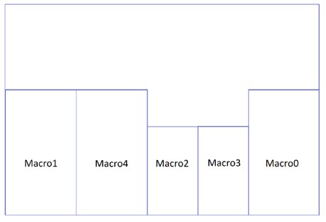
Figure 1. A: Block with fixed macros
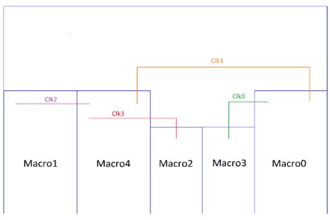
Figure 1. B: Clk* nets routing in layer metal-10(Horizontal shape) and metal-11(Vertical shape)
Macros have ESD (Electro Static Discharge) diodes that need a balanced connection to the power nets. Consider one such ESD diode that has connections to the VSS and VDD power nets while the other ESD diodes have connections to VSS and VDDH power nets. Consider two vertical shapes of VSS and VDD in metal-9, put one after the other in horizontal progression. These two vertical shapes of VSS and VDD are stacked horizontally to form an ESD diode region. You must draw the horizontal metal-10 shape of VSS at the center of the vertical metal-9 shapes of VSS and the same has to be done for VDD. This pattern ensures equal current distribution to metal-9 from metal-10 in the ESD region that is critical to its desired performance and safety.
Macro-2 in our block is the driver of Clk3. By the construction of macros, this clock pin has a single small shape in the top metal layer of macro and is surrounded by small pin shapes of power nets (VSS and VDDH). All of these power pins are internally not connected to the other power shapes of the macro. So, if we don’t connect these pins to the respective power shapes outside of the macros, they remain open and affect the functionality of the macro.
Up to some extent, the shortest path requirement can be fulfilled by default routing. But the requirement of symmetrical connection in the ESD diode region can’t be fulfilled with default routing. Deviation from its central location in the ESD region gives different current distribution to different discharge paths during an occurrence of the ESD affecting the protection capability of the diode. Default routing cannot guarantee that all shapes of one particular net in two consecutive metal layers are aligned and have proper VIA dropped between them to maintain the connectivity.
You can efficiently fulfill these requirements by custom work using a tool rather than letting the tool do it all alone.
With these inevitable stringent requirements and the need for custom work, we will go through the process of custom routing. But, before going through the process, let’s look at what information (the stringent requirements) is provided to start with.
Which information is available?
The full chip consists of many blocks but we will consider one block for our journey of custom routing learning. The area that is not occupied by the macros in the block is our core region. The block has five different macros with fixed locations and it is shown in Figure1. It doesn't matter for custom routing in our case whether the standard cells are placed and routed or not. The block has metal1 to metal11 and the AP (last layer in block) layer. The available layers for custom routing are layer metal-6 to AP over the macros and metal-10 to AP in the core region. The core region, till layer metal-9 (included), is occupied by standard cells, their routing and power shapes are handled by the PnR team. There are eight control signals and four clock signals (collectively called special nets) in the block that needs to be routed. The length/width/spacing unit is ‘um’ and that of resistance is ‘ohms’. A few images are shown with multiple colors per layer and others are shown with single color per layer for better understanding.
The block has different macros and each macro is up to layer metal-6 (differs from block to block). Metal-6 over each macro is divided into different sections. These sections have a different combination of power supplies and special net pins. The pin shapes in layer metal-6 over one macro are shown in Figure 2. Section-wise power rails are given in Table 1 and shown in Figure 3. One of the requirements is section-wise power rail density to be maintained in metal-10 and metal-11 that is given in Table 2.
We need to copy the pin geometry in metal-6, over each macro, till metal-9 and these shapes are within the boundary of the macros. Then, create a power rail and do the routing of special nets in metal-10 and metal-11, these shapes cover the macros as well as the core region. The minimum width of the power rail is 2um, 3um for layer metal-10 and metal-11 respectively and the minimum spacing is DRC allowed spacing in the respective layers.
The control signal nets need to be connected to the bumps in the AP layer. We need to place the flip-chip bumps in the AP layer in such a way that the control signal nets passing in metal-11 are near to their corresponding bump. Power bumps should also be distributed in the AP layer according to the power sections to provide robust power to the lower layers. Power shapes in the AP layer have a minimum width of 10um and minimum spacing is DRC allowed spacing in the AP layer.
Table 1: Power rail sections
| Power rails in section | |||
| Power supply section | VSS | VDD | VDDH |
| Section 1 | Y | N | Y |
| Section 2 | Y | Y | Y |
| Section 3 | Y | Y | N |
Table 2: Minimum power rail density
| Power rails in section | |||
| Power supply section | VSS | VDD | VDDH |
| Section 1 | 33 | - | 33 |
| Section 2 | 33 | 33 | 33 |
| Section 3 | 33 | 33 | - |
Table 3: Clock and Control signal parameters
| Parameters | Clk* | BT_* |
| Shielding | VSS | VSS/VDD |
| Route width | 1.9 | 5 |
| Shield width | 2.5 | 3 |
| Route to shield spacing | 2.5 | 3 |
| Max resistance | 240 | - |
| Max length | 1853 | 1037 |
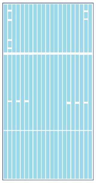
Figure 2: Pin shapes in metal-6 over macro4
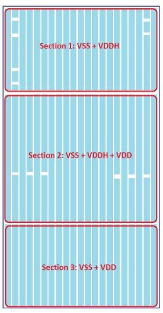
Figure 3: Section-wise power rails
The four clock signals Clk0, Clk1, Clk2, and Clk3 are connected across different macros and their routing is done in metal-10 and metal-11 layers. The eight control signals BT_0 to BT_7 need to be connected to their respective bumps in the AP layer. The routing of these control signals in the AP layer is called RDL routing. The width and spacing to be used for RDL routes are 10um. The requirements of the width and spacing of these clock signals, control signals, and their shielding are specified in Table 3.
This information is provided to us in the implementation instruction document and we must do the custom routing by keeping all these requirements in mind. With these requirements and a fixed floorplan of the block available, let’s go through the steps of custom routing in brief.
Steps
1- Copy the pin shapes in metal-6 over each macro to metal-6, metal-7, metal-8, and metal-9 as shown in Figure 4. Let the width and spacing of these shapes be as it is.
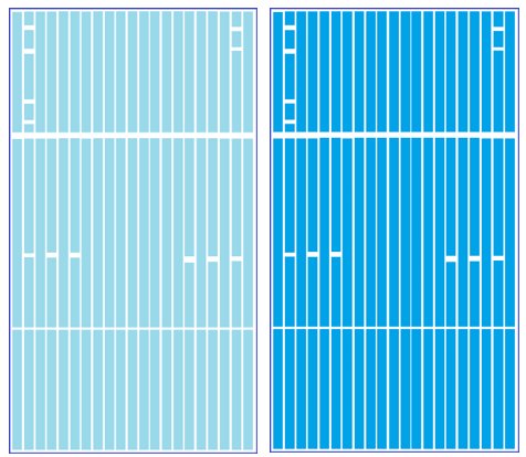
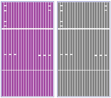
Figure 3: (a) metal-6 (b) metal-7 (c) metal-8 (d) metal-9 pin shapes of Macro4
2- Create PG shapes and that of special nets and their shielding in metal-10 as per the requirement. This is shown in Figure 5.
3- Create PG shapes and that of special nets and their shielding in metal-11 as per the requirement. This is shown in Figure 6.
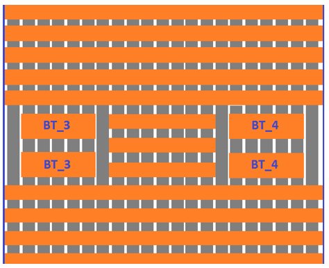
Figure 4: metal-9 (Gray), metal-10 (Orange) shapes
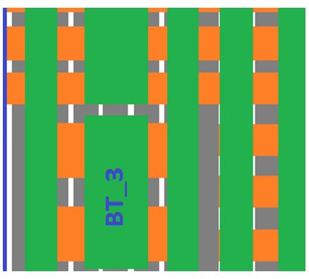
Figure 5: metal-9 (Gray) and metal-10 (Orange) and metal-11 (Green) shapes
4- The macros are located on the lower side of the block. We also need to create PG shapes in the core region that are VSS and VDD only. One major requirement that we need to take care of is continuity of the PG shapes over different sections of the macro as well as continuity of it over the core region and the macros. In the case of metal-11, it can be achieved by extending the shapes of the VSS from the upper edge of each macro (that is section 1) to the upper block boundary as shown in Figure 7. Section 1 of the macro contains VSS and VDDH but VDDH is not required in the core region. So, we can create the shape of VDD in the core region instead of extending VDDH in the core region. Similarly, the continuity of PG shapes in metal-10 can be taken care of.

Figure 6: metal-11 shapes: VSS(Blue), VDD(Purple), VDDH(Red)
5- Clock signals need to be routed in layers metal-10 and metal-11, keeping in mind that they should satisfy the maximum length requirement. The clock signal routing step can also be done before creating PG shapes in metal-10 and metal-11 or along with the shape creation of metal-10 and metal-11 and proceed accordingly. One of the possible clock signal routings is shown in Figure 8 (same as Figure 1. B).
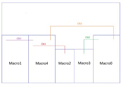
Figure 7: Clk* nets routing in layer metal-10 (Horizontal shape) and metal-11 (Vertical shape)
6- Bump placement in the AP layer needs to be done. One of the possible bump placements is shown in Figure 9.
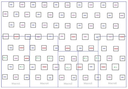
Figure 8: Bump Placement in AP layer
7- The next step is to do the RDL routing of control signals in the AP layer. RDL routing can be done by the tool automatically by specifying our requirements or it can be done manually also. But you must first do the RDL routing using the tool command and then if there are any minor changes required, they can be done manually. Figure 10 shows bumps with RDL routes.
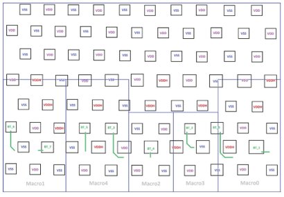
Figure 9: Bump Placement with RDL routes in the AP layer
8- Till now, we have placed the bumps and RDL routes in the AP layer. The remaining space in the AP layer has to be filled by PG shapes that cross over their respective bumps i.e. VSS, VDD, and VDDH shapes crossing over VSS, VDD, and VDDH bumps respectively. These shapes are extended in both the horizontal and vertical directions in such a way that power shapes in metal-11 are covered by their respective power shapes in the AP layer and it is shown in Figure 11.
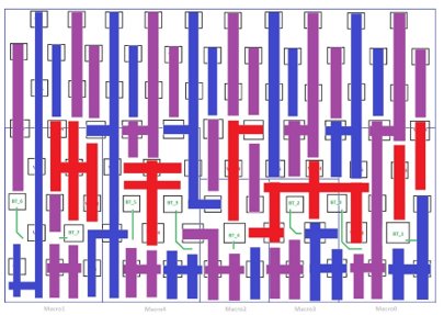
Figure 10: AP layer: VSS (Blue), VDD (Orange), VDDH (Red), RDL (Green) shapes
9- The shapes are created from metal-6 to AP. One important step is to drop the VIAs between these layers. Consecutive VIA dropping from metal-9 to metal-6 must be done only over the macro regions and not in the core region. The core region is occupied by the PnR team till metal-9. VIA dropping from AP to metal-9 has to be done over the entire block.
10- The final step is to verify different requirements like maximum resistance, maximum length, power rail densities, and the open/shorts/floating nets in the block. Practically, the custom routing requires a few iterations of the above-mentioned steps.
11- The total resistance of any particular net can be found by the report_parasitics command. Remember to check the unit of resistance before coming to any conclusion. In our case the unit is kilo-ohms.
âž” report_parasitics Clk1 -significant_digit 5
The net is ideal
RC network for net Clk1
RC corner id:0
Number of elements = 53 capacitor + 52 resistor
Total capacitance = 0.964
Wire capacitance = 0.758
Total resistance = 0.219
Wire total RC = 0.166
The net length can be found by the following command. The unit is um.
âž” get_attribute [get_nets Clk1] route_length
1707
12- Section-wise power rail density can be checked using the following proc that needs the coordinates of the section and net for which you want to calculate the density and metal layer in which you want to know the density of the specified net as an input to it.
proc pg_density {region layer net} {
set rg_shapes [get_shapes -within $region -intersect $region -filter "layer_name==$layer && net.name==$net"]
set not_area [compute_area -objects [compute_polygons -objects1 [create_poly_rect -boundary $region] -objects2 [get_shapes $rg_shapes] -operation NOT]]
set total_area [compute_area -objects [create_poly_rect -boundary $region]]
set net_area [expr $total_area - $not_area]
set net_percentage [expr ($net_area/$total_area)*100]
return $net_percentage
}
set region {{0 651.943} {0 806.184} {209.720 806.184} {209.720 739.513} {287.065 739.513} {287.065 806.184} {495.569 806.184} {495.569 651.943}}
set net VSS
set layer M10
âž” set vss_m10_density [pg_density $region $layer $net]
33.287
Similarly, the other requirements can be checked using the built-in command or making scripts as per the requirement.
In the above-mentioned steps, we have seen the logical sequence followed to complete the custom routing. The recipe creation is also an important aspect in the efficient implementation of the above steps and to accommodate any future changes in the floorplan or any other parameters. Let’s go through a few important recipe creation methodologies. Consider section 3 of any macro, which contains VSS and VDD only. Creating shapes within this region starting from the bottom (for metal-10) and left (for metal-11) of this section is as simple as going through for the loop for a specific number of iterations. The loop contains the create_shape command of VSS and VDD net alternatively. For section 2, we need to first create the shapes of VSS, VDD, and VDDH alternatively until we reach the region where the shapes of special nets are required. Now, the special net’s shape requires careful consideration of the requirements. This shape creation requires manual measurement to give exact dimensions. Then, move on to the creation of the rest of the shapes. The same is the case for section 1 with VSS and VDDH. Continuity of power shapes needs to be maintained between the sections of a macro as far as possible as shown in Figure 7. This is how the custom routing of one macro till metal-11 is done in our case.
Another way of custom routing of one macro is explained in this paragraph. Create the recipe only for special net shape creation with design constraints for the required metal layers. Then, create a separate recipe for the PG shapes creation according to the design requirements. Source these two recipes and we would have done the custom routing of one macro.
Construction-wise Macro0, Macro1, and Macro4 are the same with a few changes. Similarly, Macro2 and Macro3 are the same with a few changes. So, the custom work done for the Macro0 and Macro3 can be reused for the rest of the macros with some changes. After integrating the recipes for all of the macros, try to have continuity of shapes at the touching edge of two macros. This requirement can also be taken care of during the recipe creation of a particular macro.
The RDL routing in the AP layer is done before the AP power shape creation. The AP shapes can be created around each bump cell by taking reference to that particular bump cell. The dimensions of these shapes need to be given manually. The reason is, as many power shapes as possible in metal-11 need to be connected to AP shapes. This makes the recipe creation for the AP layer time-consuming.
Conclusion
In the presence of the EDA tools, some tasks require more human intervention than the others and custom routing is one of them. The team provides the documentation guidelines to start with custom routing. Start with the lower metal layers and reach the AP layer as mentioned above while fulfilling the design requirements. Every step has to be executed thoughtfully to have lesser implementation iterations. The documentation guidelines like maximum resistance, maximum length, power, and special net shape’s width/spacing, and section-wise power shapes density have to be verified and it completes the custom routing process.
eInfochips – An Arrow company has been working on SoC chips and IP development for more than 15 years. While working for many customer projects in the field such as ethernet switches, data center storage, cloud computing, and consumer application, etc. eInfochips has developed many Proof-of-concept in physical design implementation flow to help achieve faster time to market and bug-free designs to its customers. To know more about our expertise please contact our experts today.
About the Authors
Chirag Maniya
Chirag Maniya is working as Technical Lead in eInfochips. He has been contributing to physical design implementation of lower node technology for SoCs and IPs and worked on various complex SoCs with multi-million gate counts. He loves to mentor his juniors and enables them to contribute technically.
Hardikkumar Dhamecha
Hardik Dhamecha is working as a senior ASIC Engineer with eInfochips. He has been contributing to the physical design implementation of lower node technology for SoCs and IPs. Hardik has been instrumental in understanding and setting up various flows due to his strong knowledge from his academic background as a professor.
