Industry Articles
Understanding Logic Equivalence Check (LEC) Flow and Its Challenges and Proposed Solution-March 21, 2022 |
By Priyambada Mishra, eInfochips
Introduction
Logic Equivalence Check, popularly known as LEC is one of the most important parts of the ASIC VLSI design.
Formal verification techniques have been developed using mathematical proof rather than simulation or test vectors to provide a higher level of verification confidence on properties. For example, the implementation can be either a Verilog RTL module or an abstract version of a particular design, while the specification is typically a set of properties that needs to be verified and expressed suitably. So, formal verification provides a complete verification of each specification property under considering corner cases even without test vectors.
Formal verification has two different types of basic tools for checking ─ equivalence checkers and model checkers.
Equivalence checkers are used for implementation verification and the question arises: “Has my implementation been conserved during process transformations?”
Model-checking is another form of formal verification tool and answers the question: “Does my implementation assure the properties of the specification?”
In any typical SOC design, there are several tools in the flow that can perform operations on a particular design. Every step can initiate subtle modifications in the design behavior that can be missed by the simulations. Equivalence checking provides the ability to verify the consistency of a design and gives an efficient and quality design.
So, let’s look over the mathematical modeling used by this tool to verify the two designs.
Basic Mathematical model used by Equivalence checker
Initially, the idea was to use FSM (Finite State Diagram) modeling that represents the logic of design in the state diagram, but these things get exponentially big with an increased number of variables and states.
Then, there was a breakthrough on the state stable representation called BDD (Binary Decision Diagram), which is a more effective way to represent the variable flow. It can be reduced and shared between different functions. But it also gets big and ugly with many functions.
So, what we are looking for while dealing with the LEC is the logic equivalency, right?
Do we need a whole representation of the function, or can we figure out some other way to find that both the circuits in the logic cone are equal? So, the concept of satisfiability comes into the picture, commonly called SAT. It states that we just need to know for which inputs the function will give us 1 as output or what input will satisfy our function.
For example, F = X’ + Y + Z, is going to one when any of these terms is going to 1, F= XYZ’ then for getting one, 1 requires X=1, Y=1 and Z = 0. So, to satisfy the function, we have the required inputs.
Now, let us take a small logic cone, one from implementation (or revised), and one from reference (golden) design. With the help of the above principle of SAT, we can check for which inputs the two cones are equal or not by just adding some small logic at their output.
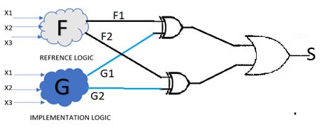
So, here F represents the reference logic and G represents the implementation logic, both with the same inputs. Now, both have two outputs F1, F2, and G1, G2 and that needs to equal for all inputs combinations available. So, we passed them with XOR gate and if they are different then it will give us 1, and then we are Oring them, which means if any of them is 1, our logic equivalence for specific inputs pattern is failing. So, what it states is that if the ‘S’ is satisfiable for any inputs, then for us the two logics are different.
This is just the tip of the iceberg of how computational Boolean algebra is powerful for making things simple that we no longer require full FSM (Finite State Machine)/BDD (Binary Decision Diagram) representation of the F OR G function. There are lots of different data structure representations and optimizing algorithms used to satisfy each specification of tools. Imagine the complexity that millions of input variables and millions of logic instances need to verify so that there is a smarter way to tackle that by dividing every big problem into smaller parts and applying recursion.
Formal Verification Flow
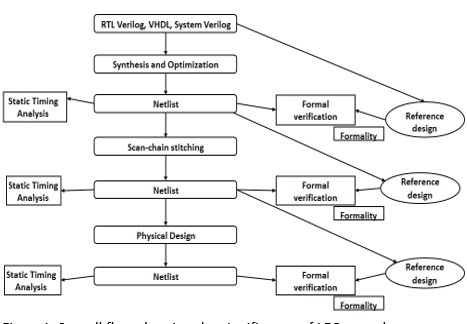
Figure 1: Overall flow showing the significance of LEC at each step.
As shown in the above flow, we can understand the significance of the LEC at each step. Once formality proves the equivalence of the implementation design to a known reference design, we can consider the implementation design as the new reference design. Using the following technique, the regression testing time of the overall verification is reduced. While working for an entire design methodology and then verifying the sign-off netlist against the original RTL (Register Transfer Level) can result in difficult verifications and can increase the duration of overall verification tests.
As shown, there are many stages where the LEC is used but the flow inside each formal verification step is almost the same. We will walk through this flow with the challenges and solutions. We focus on the challenges faced at the synthesis and the DFT scan chain insertion level. We also talk about the reasons which can fail the LEC at the physical design level. Let us jump to the detailed steps that the LEC tool performs to verify the reference and implementation designs.
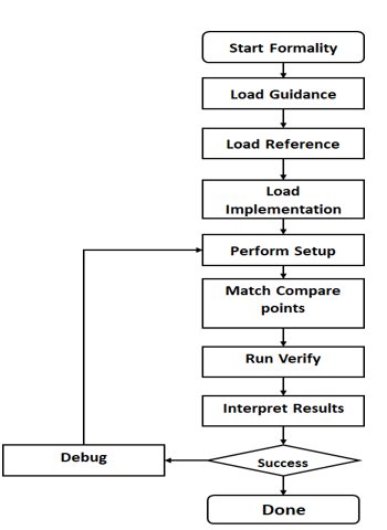
Figure 2: Steps that LEC performs for design verification.
We will go through the main steps that a user has to follow to implement the correct verification of the design.
1. Loading guidance:
Guidance helps the formality to understand and process design changes made by various tools that are part of the design flow. Formality then uses this list of information to assist in compare point matching and correctly setting up verification without user interference. It eliminates the need to manually enter the setup information, a task that is time-consuming and liable to cause an error.
Much information is passed from the synthesis tool to the formality in the form of guidance like:
- Handles undriven signals like synthesis
- RTL interpretation like synthesis
- Auto-enable clock-gating and auto-disable scan
- Multibit flops information
All this is required for the successful verification of the design by guiding the verification process. To provide such information, we need to set the automatic setup mode. Using this app variable synopsys_auto_setup, set it to true. Once the SVF is read, use report_guidance to check what and how much guidance is accepted, rejected, unsupported, and unprocessed.
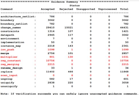
Figure 3: Report guidance
Here is an example of the rejection of the guidance for the inversion push and dropping of the multibit merging guidance. So, it is crucial to check the guidance that is dropped and find out the reasons for dropping.

Figure 4: Guidance drop at inversion push.
2. Loading the reference and implementation design:
It is a very simple step in the flow that just requires the user to load the reference design and the implementation design. Design can be loaded in .v or .ddc format, technological libs can be loaded in the form of libs, db., and ndm formats.
It is usual for one container to occupy the reference design while another occupies the implementation design. A container includes a set of related technology libraries and design libraries that entirely describe a design that is being compared against another design. In general, to perform a design comparison, you should load all the information about one design into a container (the reference), and all the information about the other design into another container (the implementation).
3. Performing setup:
It is the most important step in the LEC flow, most information needs to pass through the LEC tool before performing matching and verification. As mentioned, some of them that are dependent on the previous tool like Synthesis (Fusion Compiler), are passed in the form of guidance. But the remaining information about the black box, scan connectivity, UPF related constraints, and timing loop cut points is provided in the setup step.
4. Matching compare points:
A compare point is defined as the design object that is used as a combinational logic endpoint while doing verification. A compare point includes an output port, latch, register, net driven, or black box input pin by multiple drivers. Before design verification, formality tries to match each primary output, black box input pin, sequential element, and qualified net in the implementation design with a design object in the reference design from which it can compare.
5. Verification:
During verification, formality allocates one of the five types of statuses for every compare point it figures through verification: Passing, Failing, Aborted, Unverified, and Not Verified. Multiple reports are generated after the LEC completion like non-equivalence.rpt, failing_points.rpt, black_box.rpt, SVF guidance rpts, unmatched_points.rpt, undriven_nets.rpt, multidriven_nets.rpt, and implementation_loops.rpt. The verification failure analysis is done using the analyze, pattern viewer, and logic cones.
LEC Common issues:
- Design Read – due to reading/linking libraries or designs issues
- Match – incorrectly matched compare points, unmatched compare points, rejected SVF commands, scan mode not disabled
- Verification – clock-gating circuitry not recognized, logic differences
- DFT constraints missing
- Due to ECO implementation (Functional)
- Guidance file missing (like MBB name change in impl. design wrt ref. design cause failure)
LEC issues faced:
1. Black box inference (BBPin):
A black box is represented as a logic whose function is typically unknown. Black boxes verification failures include input pins that become compare points in the design verification. If black boxes present in the reference design do not match those in the implementation design, the compare points are not matched. In addition, compare points mismatch can occur if black box buses are not interpolated in the same manner. Issues with the black box can be due to the empty design module and due to the macro db/lib missing. Now, let us check which of them will fail the LEC.
a) Black box due to empty design:
As we compare the RTL and Synthesized netlists, we can see in the below figure that the black box is present in the reference (RTL) design while it is not present in the implementation design (Synthesized) due to which we are getting the unmatched pins of the black box. These unmatched points will eventually also fail at the verification stage as shown in the below figure:

Figure 5: Showing the verification failing points due to black boxes.
This report shows two black boxes: ONE “WDATA” that is there in the mismatched compare point. Another is of ISOLATION cells “*ISO*” that is present because of the unmapped isolation cells.
b) Black box due to macro missing dB: As this black box is inferred in both the implementation and reference designs, it is an identical black box having the pin inference in the same direction and of the same width. Thus, it gets passed in the matching point comparison.
The solution to evaluate the black boxes:
- Check the black box inference in both designs.
- Find the reason for the black box inference either it is valid, or any setup information is missing.
- Validate the identicality of black boxes in both designs.
- Provide extra information needed to resolve the black box un-matching points like port/pins direction, removing the black box from the verification.
2- DFF pins
a) Flops going into power downstate: This may happen because of verifying a partial PG connected RTL vs partial PG connected netlist. Formality by default converts the TECH cells to their power-aware models and looks for supply drivers to decide the state of the std cell/macro.
Solution: Using the “hdlin_allow_partial_pg_netlist” variable before reading in the netlist ensures mixed usage of power-aware and non-power-aware cells in the absence of UPF.
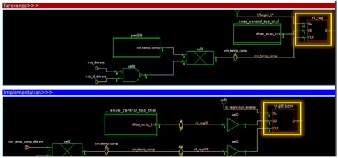
b) Clock gating issue: After synthesis, in which early clock gating is done if the setup is not done for clock gating. Then it might come into the unmatched report. The reason is obvious, the logic in the clock input of the register bank has changed and with this, the register bank compare points will go futile.
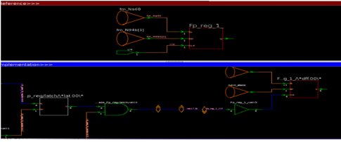
Figure 6: Showing logic cone for the clock gating failure.
3. Timing loop cut point addition (Loop): To specify the cut points for breaking combinational feedback loops, use the ADD CUT POINT command. If you do not use this command and combinational feedback loops exist, the tool will automatically add cut points on the loop combination element.

Figure 7: Logic cone for the combinational loop.
If the cut point does not match between the reference and the implemented design then it gets considered in the unmatched points and the verification fails at those endpoints. So, to fix it, we need to provide cut points as a setup for both designs.
4. UPF issues:
This includes many things like:
- Connect supply nets are missing for power domain or black boxes.
- Two power switches driving the same supply net (multi-driven nets).
- Poorly written port state.
- The port direction mismatch between the UPF and the netlist.
Low power libraries may contain cells that have incorrect or incompletely modeled power behavior. We can always check this before moving for the verification.
- Unread power/ground pins
- Missing power-down functionality on flip-flops or output pins
- Inconsistent pin directions
- Missing or invalid switch function
Conclusion:
This paper introduces logical equivalence check, flow setup, issues, and solutions to fix the LEC. We have covered some conceptual working for the LEC tool at the Boolean computational level. With reference to the Synopsys Formality tool, we covered the basic flow for the LEC, and major challenges faced between RTL and Synthesized scan inserted netlist. Also, included are the issues for power-aware verification. The demand for high performance, low power consumption, and low form-factor designs has dramatically increased in the past few years.
With 25+ years of experience, eInfochips helps its client in digital and mixed signal ASIC design, FPGA-SoCs development for various industries, including AI-driven datacenters, Aerospace, Automotive, Networking, Consumer Electronics, Industrial, Medical, IoT, etc… With strong expertise in Mixed-signal solutions across design, verification, physical design, and validation, eInfochips specializes in lower geometry designs and have taped-out 200+ silicons, from 180nm to 7nm & beyond.
About the Author
Priyambada Mishra works as an Engineer at eInfochips. She holds a Bachelor of Technology degree in Electronics and Communication from Charotar University of Science and Technology, India. With over 2.6 years of experience in lower technology node complex SOCs, she has developed expertise in Synthesis and RTL sanity checks.
References:
https://spdocs.synopsys.com/dow_retrieve/S-2021.09/dg/forolh/Default.htm#forug/pdf/forug.pdf
https://www.synopsys.com/news/pubs/snug/2018/india/ta2-03-kumar-pres-user.pdf
