By Robert Nawrath, DCD
Introduction
Electronics is everywhere, especially these days. Many times, as frequent users, we do not even notice a “paradigm change” in the things we use on regular basis. We use a fridge, but we do not care that there is a microcontroller and a set of sensors instead of a basic thermostat. We use a tablet with a touchscreen, but we do not care how the screen tap information is transmitted to the microcontroller. We use SD cards to store photos and movies in our smartphones, cameras, and other portable devices, but the card’s interface is a big mystery for many - at least for those who have never dug into the details.
Every electronic device must be equipped with a microcontroller – also called, the device brains. A microcontroller (MCU or Microcontroller Unit) is a tiny computer fabricated on a single chip. It contains at least one Central Processing Unit (CPU), memory, and input/output peripherals. When we talk about peripherals, SPI becomes crucial here – not only because of the topic… The SPI plays an essential role enabling fast, reliable, and simple short-distance communication. It is also simple enough to implement and has a low resources usage. This is reflected in the statistics: EE Times Asia article shows the most popular Microcontrollers [https://www.eetasia.com/10-best-microcontrollers-on-the-market-for-2021/]– and each and every one of them is equipped with SPI controller; the same in electronics-lab.com ranking [https://www.electronics-lab.com/top-10-popular-microcontrollers-among-makers/] and other rankings. So, it’s obvious that SPI is a must for every MCU.
This article focuses on the most important details of the modern SPI interfaces, which are improved by many useful features. But to start, let us discover the history of the modern SPI interface, because even the old, most basic SPI interfaces are still in use.
Brief history
Serial Peripheral Interface has been developed by Motorola in the 1980s. It is a synchronous serial communication interface used in embedded systems. The Single SPI specification (the first specification) describes the Master-Slave architecture (full-duplex), typically with one Master device and multiple Slave devices. It is also called the four-wire serial bus:
- SCK – Serial Clock Line (Master output)
- nSS – Slave Select line, active on low logic level (Master output, one for each underlying Slave)
- MISO – serial data line: Master In Slave Out (Master input, Slave output)
- MOSI – serial data line: Master Out Slave In (Master output, Slave input)
Why did SPI become so popular? Mainly because of its simplicity. There are no start nor stop bits, no parity like in UART bus, it enables higher transfer rates than I2C. There are plenty pros.
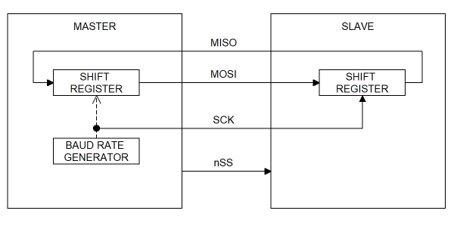
The logic resources needed to implement SPI interface are very small – Single SPI simultaneous transmission and reception synchronized by serial clock can be modelled as two shift registers in a loop, as it has been presented below:

Figure 1. SPI concept model
In reality, the SPI controller internal architecture is much more complicated than it has been shown in Figure 1, featuring more control registers, port control logic and interrupt control. The example architecture can be found in Motorola’s SPI standard – “SPI Block Guide”.
The clock phase and polarity are configurable. There are four transfer formats available:
| CPOL/CPHA | 0 | 1 |
| 0 | SPI MODE 0 | SPI MODE 1 |
| 1 | SPI MODE 2 | SPI MODE 3 |
CPOL defines, whether SCK is Low (0) or High (1) when bus is idle (nSS is High).
CPHA defines, whether first (0) or second (1) SCK edge after nSS has been asserted (nSS is Low) is used to sample data.
If data is sampled at the rising SCK edge, then shift occurs at the falling SCK edge.
If data is sampled at the falling SCK edge, then shift occurs at the rising SCK edge.

Figure 2. CPHA = 0

Figure 3. CPHA = 1
The shift registers are both 8 bits (in Master and in Slave). Data is shifted out with most significant bit first and shifted in with least significant bit first. The transmission is full duplex because both Master and Slave send and receive data simultaneously.
MISO and MOSI lines can be combined into one bidirectional line, but the transmission will be reduced to half-duplex. In this case only three wires are needed for the SPI transmission/reception.
There are many implementations of SPI bus controllers available on the market. Just as an example, DCD-SEMI’s DSPI – is a fully configurable SPI master/slave device. It is flexible enough to interface directly with numerous standard peripherals like memories, sensors etc. The IP is easy to use and utilizes a low amount of logic resources. Just as the SPI should be.
Multi line SPI
SPI is frequently used in communication with serial memories. The memory size can be large, which enforces the need of faster transfers. SCK cannot increase infinitely, so the first thought is to increase the number of data lines, not to unnecessary increase the number of wires. it is better to stay with the half-duplex transmission.
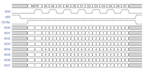
As the first - DUAL SPI has been introduced. MOSI has become SIO0 (Serial I/O 0) and MISO has become SIO1. SIO0 carries even bits and SIO1 carries odd bits. The bus throughput becomes doubled.
Then the QUAD SPI has been mastered. New data lines have been added - SIO2 and SIO3. The bit transmission scheme looks as follows:

Figure 4. DUAL and QUAD SPI bit sequence
The bus throughput becomes doubled again, and each data byte can be sent in only two SCK cycles.
The SPI transfer from/to serial memory consists of several phases: Instruction (command), Address, Data and optionally Checksum. Some commands require to be sent in SINGLE SPI mode, while ADDRESS and DATA are sent in multi-IO mode of operation.
Further extending QUAD SPI some devices increase the transfer rate by using Double Data Rate (DDR) transmission, where data lines are sampled both on the rising and falling edge simultaneously, so every data byte is sent in just one SCK cycle. An example is shown in Figure 5.

Figure 5. DDR QUAD SPI transfer
One could ask: if we are already using four data lines, why not expand further? So thought the engineers and introduced OCTAL SPI. In Single Data Rate (SDR) mode one byte is sent in one SCK cycle and in DDR mode two bytes are sent in one SCK cycle. The bandwidth increases significantly. An example is shown in Figure 6.

Figure 6. OCTAL SPI DDR transfer
The transfer format shown in Figure 6. has its limitations. Instruction is sent repeated, as two bytes, to preserve even number of bytes in transfer, because sampling is done on every SCK edge. Alternatively, the command can be sent in SDR mode. Also Address and Data phases must contain even number of bytes.
By now the CPOL and CPHA settings have lost its meaning. OCTAL SPI DDR transfers are only conducted in SPI mode 0.
For HDL designers it’s common to develop backward compatible SPI Master/Slave controllers. We can see it at DCD-SEMI, where we find customer`s interest in the DQSPI that supports SINGLE, DUAL and QUAD SPI transfers, while DOSPI supports SINGLE, DUAL, QUAD and OCTAL SPI transfers. Both support DDR transfers, multiple SPI slaves, implement a dedicated FIFO memory and are available with the most common CPU bus interfaces. In SINGLE SPI mode of operation all the Motorola’s SPI configurations are supported.
eXecute In Place (XIP)
Thanks to DDR and QUAD/OCTAL transfers combined with high SCK frequency it became possible to execute programs directly from a serial memory instead of copying the program memory into RAM. The program code must be stored in non-volatile memory and the serial flash memory is cheaper than a parallel. The SPI controller in XIP mode of operation can be considered as a bus bridge: from the “CPU point of view”, it is a simple memory which can be accessed parallel, and from the “SPI memory point of view”, it is just an ordinary SPI master. The CPU read transfers are performed with zero latency, if the program is executed linear (address after address) or the jump does not cross boundary of memory page, stored in controllers FIFO memory. Also, in a typical embedded system the microcontroller does run on significantly lower frequency than the SPI controller, so the data is available immediately, even if the next memory page has to be read.

Figure 7. XIP mode block diagram
In XIP mode of operation, there is also available the regular register access to SPI controller. This mode is also used to configure the IP’s internal registers.
Typically, the eXecute In Place is used in First Stage Boot Loader, e.g., in embedded systems, in Linux OS, in BIOS etc. The SPI controller is preconfigured on power-on reset and after the reset is deactivated it starts reading the first memory page. There are also attempts to prepare file systems based on XIP.
The before mentioned DQSPI/DOSPI, as well as the latest SPI Flash Controller (DFSPI) are also available with the XIP interface. This ensures optimal system performance and wide configuration options.
Recently, another interesting feature can be found in SPI controllers, like in the DFSPI. For best performance and lowest software overhead the automatic configuration feature can be used. The SPI controller is equipped with additional small memory, which acts as the lookup table, storing predefined device configuration. The memory content is prepared before the synthesis and implementation or in more advanced solution, it can be modified like an ordinary internal register. After writing Instruction/Command into the SPI controller, the device is automatically configured. The configuration may cover:
- Command code
- Addressing mode
- Transfer type – transmission or reception
- Latency / Dummy cycles
- SPI mode: SINGLE, DUAL, QUAD, OCTAL
- SDR / DDR
- Other
xSPI – eXpanded Serial Peripheral Interface
Based on the information from this article, we can see how handy SPI is. JEDEC created a new standard above SPI, with limited backward compatibility. The standard defines commands for general purpose read and write of any device, which helps in system development. Before every manufacturer created his own set of commands. xSPI helps to develop device provider independent applications.
xSPI enables flexible configuration of SPI transfer mode (SINGLE, DUAL, QUAD, OCTAL) and SDR/DDR mode. Instruction, Address and Data can all be independently performed in one of the modes as follows:
- Instruction phase – Address phase – Data phase
- Width (number of data lines used)
- 1: SIO0
- 4: SIO0, SIO1, SIO2, SIO3
- 8: SIO0, SIO1, SIO2, SIO3, SIO4, SIO5, SIO6, SIO7
- Data rate options: S for SDR, D for DDR
For example, a 4S-4D-4D can be performed.
Just to admit, that HyperBus has also become part of xSPI in 2017. It has been named xSPI type 8D-8D-8D Profile 2.0.
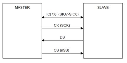
In both HyperBus and xSPI, high clock rates can be achieved by using a separate clock signal for transmission (Master generated) and for reception (Slave generated / returned with internal delay). This provides best timing reference and is source dependent. The Data and strobe must be synchronous while the strobe and SCK have no phase dependency.

Figure 8. xSPI bus lines

Figure 9. xSPI transfer

Figure 10. xSPI transfer
The DFSPI is one of the SPI controllers already supporting xSPI.
It’s worth to mention that recently a new Xccela Consortium has been established. The new standard is xSPI compliant at the physical layer. It does focus on the plug-and-play compatibility between products. It does provide complete device specifications and guidelines for designers.
eSPI – serial bus replaces parallel bus
Enhanced Serial Peripheral Interface uses the same timing and electrical requirements as regular SPI, but it is designed to replace the deprecated LPC bus which has replaced the ISA bus on the PC’s motherboard. The LPC messages and much more are replaced by in-band SPI transfers. eSPI is low power, energy efficient and configurable bandwidth bus. Even though at the physical layer the eSPI uses the same SPI bus, the protocol and requirements are different.
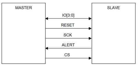
First of all, eSPI introduces a new signal “alert”, which works like an interrupt request from Slave to the Master. If the Master asks for data and the data cannot be immediately returned, the transmission is ended and the Slave requests transmission completion after the data has been prepared. Alert can only be driven when bus is IDLE (CS is high).

Figure 11. eSPI bus lines
Each eSPI transfer consists of a COMMAND and RESPONSE phase divided by a TURN AROUND phase. In COMMAND phase the MASTER drives information on the bus. In TURN AROUND all IO lines are tri-stated, and the bus mastering is given to SLAVE. In RESPONSE the SLAVE drives information on the bus. Both COMMAND and RESPONSE are supervised by CRC. In RESPONSE phase the eSPI Slave also returns the internal Slave STATUS register state.

Figure 12. eSPI transfer
Without going deeper into the details of the eSPI bus, we can see how different it is – also a good example of the usage of the SPI bus. xSPI gathers all the previous SPI standards together, while eSPI is a totally different standard. eSPI has been created by Intel and is best tailored for motherboards with Intel CPU (Intel architecture Skylake U or newer).
eSPI standard goes back to 2016. As we can see in different vendors portfolios, it is not so common like xSPI, but DCD-SEMI has already got a dedicated DESPI controller available.
Summary
SPI has evolved over last 4 decades - from a basic concept to an advanced serial bus. But one thing remains the same - it is commonly used and can be found everywhere. But before you use a SPI controller in your next project, it will be worthwhile to compare the available IP’s and to choose the one best fitting in your design. As an example, you can take a look at the table below. All SPI IP Cores, but the functionality differs. A lot.
