By Aditi Sharma, NXP
Abstract
With the introduction of advanced driver assistance systems (ADAS), complex vehicle infotainment, and high-end instrument cluster, automotive subsystems are shifting towards faster processors with increasing CPU core count year over year. CPU core counts are increasing at a rate that surpasses overall system memory bandwidth. SRAM and non-volatile memories are not enough to satisfy the high capacity and high bandwidth memory requirements needed for complex computing and image processing to support ADAS features. That is why the automotive industry is showing a growing need for DRAM every day.
But signal integrity, layout complexity, and other system-level challenges are limiting advances in DRAM bandwidth. So, it’s very important to utilize the DRAM bandwidth to the full extent. In this article, we will see which parameters we can tweak inside the DDR controller for getting optimized throughput from LPDDR4/4x DRAMs.
I. Bank rotation/interleaving
Each DRAM memory rank is organized in a BANK-ROW-COLUMN structure. When the DDR controller receives a request to read/write data into a memory location, it has to send ACTIVATE command to DRAM for opening that particular row in a bank. Once the row is opened, that row's data is copied into that bank's Row Buffer.
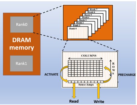
Figure 1 DRAM memory organization
When the DDR controller receives a Read/Write request for some other row in the same bank, it has to send a PRECHARGE command to close the already opened row before sending ACTIVATE command to open another row. The row-closing penalty is much higher than the Row opening penalty.
On the other hand, if DRAM has ‘n’ banks, ‘n’ rows can be simultaneously activated and accessed; one per bank.
Bank interleaving is the concept of spreading memory addresses evenly across memory banks to prevent frequent PRECHARGE and ACTIVATE requests.
It can be accomplished by System address to DRAM row-bank-column address translation provided inside the DDR controller. This translation gives flexibility to users in choosing a configuration-specific best scheme.
Broadly two types of addressing schemes are possible:
- Bank-Row-Column scheme
- Row-Bank-Column scheme
i) Bank-Row-Column Address Scheme (BRC)
In this scheme, MSBs of System address are mapped to Bank bits, Middle bits to Row bits, and LSBs to Column bits.
If the master is accessing contiguous memory locations, the row address will be changed
once all columns in that row are accessed. If there are 1024 columns in a row with each column of size 2 bytes, in this scheme rows within a bank are switched every 2048 bytes adding PRECHARGE and ACTIVATE overhead.
![]()
Figure 2 Contiguous read in BRC scheme
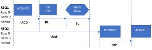
Figure 3 Row accessing time in the BRC scheme
For a 2GB 16bit data bus device with 10 Column bits, 3 Bank bits,1 Chip select, and 16 Row bits, the RBC scheme can be achieved by following address map settings:
| System address | 30 | 29 | 28 | 27 | 26-11 | 10 | 9 | 8 | 7 | 6 | 5 | 4 | 3 | 2 | 1 | 0 |
| DRAM address | CS0 | B2 | B1 | B0 | R15-R0 | C9 | C8 | C7 | C6 | C5 | C4 | C3 | C2 | C1 | C0 | - |
ii) Row-Bank-Column Address Scheme (RBC)
In this scheme, MSBs of System address are mapped to Row bits, Middle bits to Bank bits, and LSBs to Column bits.
If a master is accessing contiguous memory locations, row addresses within a bank will change once all the rows in all 8 banks have been accessed. In this case, row switching within the same bank will be done after 8*1024*2 = 16K bytes.
![]()
Figure 4 Contiguous read in RBC scheme
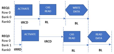
Figure 5 Row accessing time in RBC
For a 2GB 16bit data bus device with 10 Column bits, 3 Bank bits,1 Chip select, and 16 Row bits, the RBC scheme can be achieved by following address map settings:
| System address | 30 | 29-14 | 13 | 12 | 11 | 10 | 9 | 8 | 7 | 6 | 5 | 4 | 3 | 2 | 1 | 0 | |
| DRAM address | CS0 | R15-R0 | B2 | B1 | B0 | C9 | C8 | C7 | C6 | C5 | C4 | C3 | C2 | C1 | C0 | - |
In LPDDR4/4x, back-to-back masked writes within the same bank result in a performance penalty (masked writes are the write operations that include a byte mask anywhere in the burst sequence). Masked writes are most frequent when Inline ECC is used or when writing data less than the programmed burst size (BL16). After masked writing in a row, the waiting period for writing in the same row is tCCDMW.
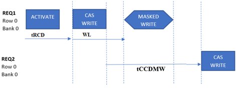
Figure 6 LPDDR4 Masked writes penalty
To mitigate this penalty, RBC addressing scheme can be further improvised into Row-Bank-Column-Bank-Column (RBCBC) scheme. In this scheme, after every BL16 burst, Bank is switched. We can use 2 Bank rotation for the same in which banks are rotated every burst with rotation between 2 banks.

For a 2GB 16bit data bus device with 10 Column bits, 3 Bank bits,1 Chip select, and 16 Row bits, this can be achieved by following address map settings:
| System address | 30 | 29-14 | 13 | 12 | 11 | 10 | 9 | 8 | 7 | 6 | 5 | 4 | 3 | 2 | 1 | 0 | |
| DRAM address | CS0 | R15-R0 | B2 | B1 | C9 | C8 | C7 | C6 | C5 | C4 | B0 | C3 | C2 | C1 | C0 | - |
iii) Choosing between BRC and RBC
As discussed in previous sections, the RBC scheme offers an advantage when consecutive DRAM locations are addressed viz. LSBs are changing more frequently. This is mostly true when a single master is accessing DRAM.
In Multi-master or completely random traffic scenarios, where MSBs may be changing more frequently than LSB, the RBC scheme may not prove to be that efficient. Since all masters share all banks, they can cause mutual interference by closing each other’s rows. In that case, private bank mapping can be tried where each master is assigned its bank or set of banks. Therefore, the state of the row buffers of one master cannot be influenced by other masters.
II. Rank Interleaving
In multi-rank devices, the row closing penalty can further be mitigated using Rank interleaving. In this scheme, rank is switched once all columns (belonging to the same row) in all banks are exhausted. Since there is no minimum timing constraint to send ACTIVATE command to another rank, another consecutive request to a different rank can be serviced immediately by the controller. There can be some Rank switching delay which is variable depending on the usage of ODT in the system. If ODT is enabled there is a slight increase in Rank switching delay w.r.t ODT disabled case.
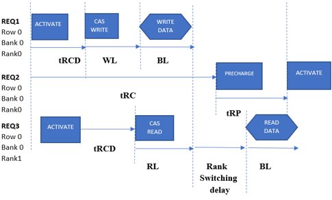
Figure 7 Rank Interleaved row access time
Another benefit of rank interleaving is that refreshes to two ranks can be staggered. If one rank is blocked for a refresh cycle in the All bank scheme, another rank can service Read/Write commands. A slight modification can be done in the RBCBC scheme mentioned in the previous section. In this scheme, rank switching happens earlier compared to row switching in case of contiguous address access from a master.
For a 2GB 16bit data bus device with 10 Column bits, 3 Bank bits,1 Chip select, and 16 Row bits, this can be achieved by following address map settings:
| System address | 30-15 | 14 | 13 | 12 | 11 | 10 | 9 | 8 | 7 | 6 | 5 | 4 | 3 | 2 | 1 | 0 |
| DRAM address | R15-R0 | CS0 | B2 | B1 | C9 | C8 | C7 | C6 | C5 | C4 | B0 | C3 | C2 | C1 | C0 | - |
III. Quality of Service (QoS)
In any SoC-based on-chip communication system, there will be multiple Masters trying to communicate with different Slaves through Interconnect. Interconnect is used to route the traffic between the Masters and Slaves. There are potential chances that high bandwidth non-latency critical masters can starve low bandwidth, latency-critical masters. This impacts the overall performance of the sub-system. QoS addresses these kinds of performance issues in the sub-system.
Based on incoming QOS from masters, the DDR controller can assign them High priority or low priority queue. Latency-critical masters must be placed in high priority queue so that their transaction requests can be serviced immediately.
To prevent starvation of masters placed in Low priority queues, timeout counters can be enabled. If a transaction is pending for some time in the low-priority queue, that transaction can be promoted to the high-priority queue.
IV. Refresh Schemes
A DRAM cell consists of a capacitor to store one bit of data as an electrical charge. The capacitor leaks charge over time, causing stored data to change. As a result, DRAM requires an operation called refresh that periodically restores electrical charge in DRAM cells to maintain data integrity. While DRAM is being refreshed, it becomes unavailable to serve memory requests. As a result, refresh latency significantly degrades system performance.
The minimum time interval during which any cell can retain its electrical charge without being refreshed is called the minimum retention time, which depends on the operating temperature and DRAM type. Because there are tens of thousands of rows in DRAM, refreshing all of them in bulk incurs high latency. That is why memory controllers send several refresh commands that are evenly distributed throughout the retention time to trigger refresh operations. Usually, the retention time of each cell at room temperature is around 64ms. There are two ways in which refresh commands can be scheduled in this 64ms time interval for LPDDR4 memory:
- All Bank Refresh Scheme
- Per Bank Refresh Scheme
i) All Bank Refresh Scheme
In this scheme, the refresh command operates at the entire rank level. Refresh commands are scheduled at time intervals of tREFIab with the duration of each refresh command being tRFCab. In each refresh command, some rows of all banks are refreshed.

Figure 8 All Bank refresh scheme[3]
When the refresh cycle is going on, no ACTIVATE commands can be sent to any of the banks. The entire rank cannot process any memory requests during tRFCab, The length of tRFCab is a function of the number of rows to be refreshed. So, tRFCab is directly proportional to device density. It should be noted that refresh commands to different banks are slightly overlapped.
ii) Per Bank Refresh Scheme
LPDDR provides a finer-granularity refresh scheme, called per-bank refresh in which All Bank refresh operation is split into eight separate operations scattered across eight banks. Therefore per bank refresh command is issued eight times more frequently that all-bank refresh commands. Refresh commands are scheduled at time intervals of tREFIpb (tREFIab/8) with the duration of each refresh command being tREFpb (tREFab/8<tREFpb<tREFab).
As per the old JEDEC standard, per-bank refresh commands were not overlapped for simplicity.

Figure 9 Per Bank refresh scheme[3]
iii) Performance comparison: All Bank vs Per Bank
Per Bank refresh scheme is performance friendly because when one bank is getting refreshed in a rank, other banks are accessible.
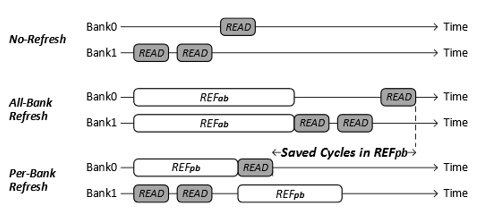
Figure 10 Performance comparison All bank vs Per bank[3]
But a per-bank scheme can only be used when certain conditions are met. Those conditions are discussed in a later section.
Apart from choosing the right refresh scheme, DDR controllers also offer a programmable field to postpone the refreshes. At nominal temperature, up to eight all-bank refreshes can be postponed and up to sixty-four per-bank refreshes can be postponed. When a large burst of read/write is ongoing, this postpone feature can prevent closing pages in between transactions when a refresh is due thus improving performance slightly.
V.Intelligent Page Policy
There are two ways in which we can choose to PRECHARGE a row within a bank.
- Closed Page Policy in which a row is closed immediately after the transaction
- Open Page Policy in which row remains open until there is a need to close it (Either a refresh cycle is due for that bank or another row within the same bank needs to be activated).
Both the above policies have advantages and disadvantages.
In the case of the Closed Page Policy, if the next transaction is also on the same row, an extra overhead of opening the same row again is added. The advantage of this policy is that if another transaction is on a different row, the row closing overhead before opening the new row is avoided.
Open Page Policy is the complement of the first policy. The advantage offered by the first policy is the disadvantage of the second policy and vice versa.
So, DDR controllers nowadays offer a midway approach trying to extract the best from both of the policies. This midway approach is called Intelligent Page Policy.
In this case, a row is kept open while there are page-hit transactions available in the local command buffers to that row. The last read or write command in the local command buffers for that row is executed with auto-precharge.
VI. Performance degradation with temperature
As DRAM temperature increases, DRAM cell retention time decreases because the capacitor loses charge more quickly. To mitigate this, refresh cycles need to be sent to DRAM more frequently. As temperature rises above the nominal temperature (85 degrees) refresh interval is reduced to 0.5x and 0.25x. The refresh command which was sent earlier every tREFIab in case of all bank refreshes is now sent every tREFIab/2 or tREFIab/4. The same is true for per bank refresh.
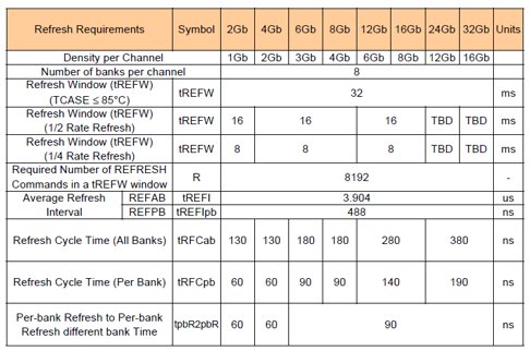
Figure 11 Refresh variation with Device density and Temperature[2]
As long as tREFI/4 is greater than tRFC, there is no issue. But when tREFI/4 < tRFC, a problem arises because the interface will be blocked for refresh forever. This is because we can’t send any ACTIVATE command to a bank if tRFC is not elapsed or the next refresh is due. At high temperatures, both conditions are never met if tREFI/4 < tRFC.
For Devices with Density per channel >=6Gb, this problem arises in case of Per bank refresh. For DDR controllers and DRAMs compliant with JESD209-4A, there is no other alternative other than to use an All-bank refresh scheme for these densities.
JESD209-4B offers a solution for this limitation. We saw earlier that per-bank refreshes are not overlapped in JESD209-4A. The minimum time for completion of per bank refresh on one bank as well as the minimum time for sending per bank refresh to another bank was tRFCpb. As per JESD209-4B, the minimum time for completion of per bank refresh on one bank remains tRFCpb but the minimum time for sending per bank refresh to another bank is reduced to tpbr2pbr. Tpbr2pbr is such that it is always less than tREFI/4.
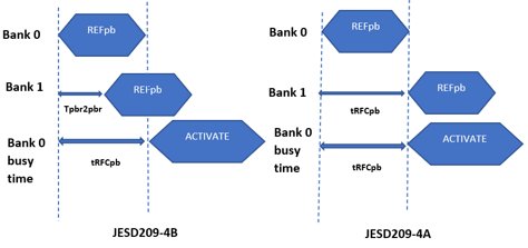
Figure 12: JEDEC restrictions on Per Bank Refresh
On JESD209-4B compliant devices, we should always opt for a per-bank refresh to get better throughput.
Apart from the above considerations, it’s very important to enable the Derating feature inside the controller. Derating automatically adjusts the refresh and other timing parameters according to DRAM temperature.
Users can choose a nominal value for refresh and other timing parameters. The controller increases the refresh frequency when the temperature increases and decreases the refresh frequency when the temperature becomes nominal again. So, the performance penalty is limited only to high temperatures. At less than or equal to the nominal temperature, performance will be increased automatically.
Derating is achieved by continuous polling of the MR4 register present inside DRAM. As per the expected temperature gradient of the system, the user can program the correct MR4 polling frequency inside the DDR controller.
For example, if TempGradient is 10°C/s and the SysRespDelay is 1 ms:
(10°C/s) x (ReadInterval + 32ms + 1ms) ≤ 2°C
In this case, ReadInterval should not be greater than 167 ms.
Polling frequency should not be kept unnecessarily high.
VII. Performance vs Power Savings
LPDDR4 uses an I/O signaling scheme known as low voltage swing terminated logic (LVSTL).
The advantage of this signaling scheme is that it consumes no termination power while a low level (0) is being driven through the I/O drivers. Power is consumed only while transmitting 1’s.
A power-saving feature called Data Bus Inversion is introduced which aims at minimizing the number of 1’s in a byte. This is done by inverting each byte of read or write data if the number of 1’s in that byte is greater than 4. A DBI signal (1 bit per byte of data) is used to indicate to DRAM whether this has been done or not.
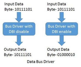
Figure 13: LPDDR4 Data Bus Inversion
Though DBI offers power savings it hampers DDR performance especially read performance.
This is because Read Latency cycles are increased when DBI is enabled. Many other timing parameters which are a function of Read Latency have to be increased.

Figure 14: Latency Cycles comparison with DBI[4]
So, we have to check whether our system’s focus is on Performance or better power saving. Depending on that we should keep DBI enabled or disabled.
References
[1] Tackling Roadblocks to Achieve Optimum DDR Performance
[2] JESD209-4B
[3] Improving DRAM Performance by Parallelizing Refreshes with Accesses
[4] Automotive LPDDR4/LPDDR4X SDRAM Datasheet
