By Nadim Mansuri, Vrushabh Vakhare, and Kashish Shah eInfochips – An Arrow Company (Ahmedabad, India)
Introduction:
This article discusses the power analysis of a complex 7nm networking chip. As the next-generation System on a Chip (SoC) moves toward the future, the chip size decreases with a simultaneous increase in the number of switching transistors to meet the demand for better functionality. A proper design analysis mitigates risks, accelerates time to market, and thus provides the best design qualities of power, performance, area, and reliability.
The phenomenon of voltage drop occurring at the metal wire grids, just before the power pins of standard cells, is commonly referred to as IR drop. It arises due to the resistance encountered by the metal wires and the current flowing through them.
Effectively managing the IR drop is of utmost importance in the chip design as it significantly impacts various aspects of the chip's performance. Let's explore how the IR drop influences different factors:
- Power: IR drop directly affects the delivery of power to the cells within the chip. When metal wires possess higher resistance, it leads to a greater voltage drop, thereby reducing the voltage available for the cells. Consequently, this can result in functional failures, increased power consumption, and performance degradation due to a decrease in the power supply voltage.
- Performance: IR drop has implications for the timing and overall chip performance. If the cells’ voltage decreases significantly due to a substantial IR drop, it can result in slower switching speeds and an increased signal propagation delay. These factors can adversely impact the chip's operating frequency and response time, affecting its performance.
- Area: To mitigate IR drop, designers often resort to adding more metal layers or widening the wires, which can occupy a wider chip area. This increase in area utilization can impact the overall chip size, potentially limiting space for other essential components or functionalities.
- Reliability: Excessive IR drop can generate reliability issues. Insufficient voltage in the cells can lead to functional errors or even permanent damage to the chip. It can manifest as timing violations, signal integrity problems, and an increased susceptibility to noise and electromigration, compromising the chip's reliability.
To address these concerns and restrict IR drop, chip designers employ several techniques, including:
- Power Distribution Network (PDN) design: Optimizing the layout of the PDN, such as carefully positioning power and ground rails, incorporating decoupling capacitors (De-Caps) in high density regions, and implementing effective power grid structures, aid in minimizing the IR drop.
- Clock and power gating: Intelligently gating or shutting down power to specific sections or inactive portions of the chip can reduce power consumption and subsequently mitigate IR drop.
- Signal integrity analysis: Conducting meticulous analysis to identify critical paths and regions with high currents helps optimize routing and mitigate the IR drop effects.
- Current-aware Floor planning: Thoughtful floor planning, considering power delivery requirements, and minimizing long wire segments, assist in mitigating IR drop.
- Voltage drop analysis and optimization: It is necessary to look out for high density regions in the design where cells having higher driving strength are clumped together. This is done by making proper adjustment in the PNR flow through cell spreading, applying keep-out margin to cells which are closely placed or have high pin density in that area. Applying proper clock cell spacing also helps avoid potential IR issues.
In advanced technology nodes, along with the transistor size, the metal wire dimension is also scaled down. It results in increased metal resistance, making it a dominant factor at the lower technology node. This scaled wire dimension and wire resistance lead to IR drops and electron migration. Both effects can lead to the functional failure of the design.
At the lower technology node, dynamic current density increases as transistors are physically much closer to each other in every direction. Decreasing the distance between transistors leads to heat trapped between the fins. Also, at lower technologies, the node leakage current increases. Both effects can lead to metal migration.
Overview of Static IR, Dynamic IR and Electromigration
The power delivery network experiences a voltage drop, which is a static IR drop, when there are no input transitions or switching taking place. The voltage loss in the power supply network caused by continuously switching inputs is referred to as dynamic IR drop. The key problem with an IR drop is logic-dominated blocks, where we might need to cut back on our PG routing resources.
The movement of atoms depending on the transfer of electricity through a material is known as electromigration. The heat generated inside the material repeatedly separates and moves atoms if the current density is high enough. Both "deposits" and "vacancies" result from this. While deposits can develop and eventually close circuit connections to cause short-circuits, vacancies have the potential to expand and finally destroy circuit connections, resulting in open circuits.
Challenges encountered in our design:
To ensure accurate data and a clearer picture of the analysis' conclusions, adjustments and alterations were made to the IR workflow. Here are some possible modifications that could be implemented, and we will discuss both workflow adjustments and physical design methods in this article to overcome the IR.
Case 1: MIM Cap calculation in IR analysis –
MIMCAP (Metal-Insulator-Metal Capacitor), which has parallel plates, is constructed from two metal sheets. There is a thin insulating dielectric layer in between the capacitor’s top metal (CTM) and bottom metal (CBM) layers. These MIM layers are made of Al, AlCu alloys, TiN, Ti, TaN, and Ta. The dielectric layers are made of silicon oxide or silicon nitride.
MIMCAPs are used to provide decoupling capacitance, which reduces supply noise and minimizes the negative effects on the power grid. They are placed between metal layers 14 and 15 in 7nm technology.
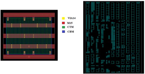
Figure 1 single MIM cap-layer wise information and MIMCAP structure for block levels
To consider the MIMCAP effect by the IR analysis tool, the CTM and CBM layer information must be present in the DEF file, and thus, MIMCAP information is a special case that requires us to first generate an IR model file to consider the MIMCAP effect.
Using the redhawk-sc tool utility gds2rh, we must produce detailed extracted LEF and DEF to account for the MIMCAP's impact.
IR’s tool (gds2rh) requires the following files as inputs to extract MIMCAP LEF and DEF:
- MIMCAP GDS
- Apache technology layer map file
- MIMCAP LEF
LEF and DEF information is extracted into an output, which is then utilized as an input by the IR tool to account for its effect.
Case 2: IR flow fixes –
Analyzing IR drops is more efficient and quicker, but a guided flow is essential to match the capability of the tool. The situation is regarded as an issue when it is found that the frame length and analysis duration are not aligned with the block-level clock frequency.
A frame length is a single value for which we create scenarios and apply 20% activity (20% of total block instances are switching at that time frame). In the next frame we select another 20% of the remaining 80%, and so on.
analysis_duration = 10*2*clock_period_value, and frame_length = 2*clock_period_value,
Detailed Explanation:
Certain information needs to be defined in the IR flow, such as analysis duration, frame length, and clock period, which are hard coded and produce sporadic or unreal results from the IR tool. As the clock period is unmatched with the actual block level period, the timing frames that the IR flow utilizes are not multiples of the analysis duration. This analysis duration is calculated from the actual block level period that was hard coded earlier. For each separate frame, the IR flow creates scenarios based on 20% actively switching instances. Thus, after completing 100% analysis, the IR flow tries to calculate the IR drop for those unmatched extra frames and ends up with sporadic results every time it runs.
Let's say, the actual clock_period_value = 0.835 ps, then analysis_duration = 16.67 ps (as per the calculation).
And the frame_length = 1.25ps (hard coded)
Therefore, IR flow's “cell type-wise coverage” would take a total of 16.67/1.25 = 13 frames for analysis. So, if only 20% of instances are switching at a time, then it would have completed 100% in just 5 frames, and with 13 frames, the analysis would have occurred twice, and would restart for the remaining 3 frames and end up with just 60% of analysis. Thus, IR counts are sporadic and cannot be determined whether they get fixed or not after the implementation of the Engineering Change Orders (ECOs).
The problem gets fixed with the change in frame_length value:
Necessary changes must be made in the IR flow’s dynamic.py file as mentioned below:
The specific changes mentioned are related to the functions scenario_utils.get_switching_coverage() and scenario_utils.get_power_data().
scenario_utils.get_switching_coverage(scn_no_prop_vectorless, file_name=reports_dir+'/npv_switching_coverage.rpt', frame_length=2*clock_period_value)
scenario_utils.get_power_data(scn_no_prop_vectorless, file_name=reports_dir+' /npv_power_data.rpt’, frame_length=2*clock_period_value)
Now, frame_length = 2*clock_period_value = 2*0.835 ps = 1.667 ps, and analysis_duration = 16.67 ps, which is in multiples, and even if analysis occurred twice or thrice, the complete analysis of all block-level instances would have been taken.
Table 1 Comparison
(Analysis results before and after the IR flow update)
The data above mentions the analysis results before and after the IR flow update. With the default flow, the data IR and clock IR results show random violation counts every time the flow is executed, regardless of any Engineering Change Orders (ECOs) made to address specific IR violations. The violation counts do not decrease consistently. However, after the flow fixes (presumably after making the necessary changes mentioned earlier), the results seem to be more comparable, suggesting that the flow improvements have addressed the sporadic violation counts and produced more reliable results.
The run time taken by the IR tool for larger blocks (having a higher instance count) drastically decreases, helping in the flow run completion for other blocks with the fewest licenses.
Physical design methods to overcome IR at ECO stages:
- Downsizing instances would be helpful if there is no timing violation through it and if IR violations are in large count, then preparing TCL scripts would be advantageous.
- Spreading the instances having higher driving strength placed together or sharing the same voltage domain area.
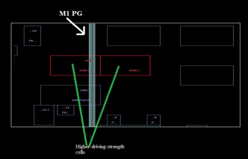
Figure 2: Higher-driving-strength cells sharing the same voltage domain.
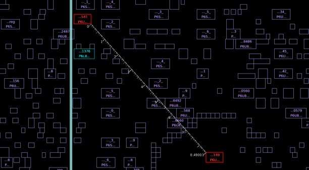
Figure 3: Both higher driving strength cells are moved away to mitigate IR drop.
- Moving instances having high driving strength away from memory regions.
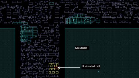
Figure 4: The above picture shows a red-colored IR-violated cell placed near the memory region and surrounded by yellow cells having higher driving strengths of X28, X32, and X40.
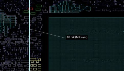
Figure 5: Red colored IR cell moved with respect to M1 PG routing.
To solve such a problem, the violated cell is moved away from the memory channel, where the cell density is lower, and the surrounding flops also have low driving strengths of X2 and cells with X1 strength. While moving a violated cell, make sure the availability of the PG rail is near that cell.
- Providing extra VDD/VSS source near the violated instance by creating PG rails and dropping VIAS near to it.
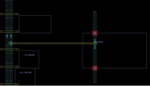
Figure 6: Manual creation of P/G rail and dropping M0 P/G via to mitigate IR drops.
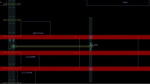
Figure 7: Manual creation of P/G rail and dropping M0 P/G via to mitigate IR drop with a clearer picture of site row at layer M0
About Authors:
|
| Nadim Mansuri is working as an ASIC Physical Design Engineer at eInfochips (An Arrow Company), Ahmedabad, India. He has more than 4.5 years of experience in Physical Design. He has worked on nodes as different as 90 nm, 22 nm, 16 nm, 7 nm and 5nm. His main area of expertise is networking ASICs. He has handled blocks with multimillion instances that are memory, power, and congestion critical. |
|
| Vrushabh Vakhare is working as an ASIC Physical Design Engineer at eInfochips (An Arrow Company), Ahmedabad, India. He has 2 years of experience in Physical Design. He has experience with the ASIC project at the 7nm/5nm technology node. He worked with timing, power, and congestion critical multimillion-instances-blocks. |
|
| Kashish Shah pursued Electronics and Communication from LD College of Engineering, Ahmedabad and is serving eInfochips – An Arrow Company as ASIC Physical Design Engineer for the last 2 years and is experienced in working at 7nm/5nm lower technology node. He is experienced in handling PPAC. critical blocks from PNR to signoff stages (DRC, LVS, ANT). |


