Industry Articles
The complete series of high-end DDR IP solutions of Innosilicon is industry-leading and across major foundry processes-December 22, 2023 |
By Innosilicon
In recent years, emerging industries such as AI, Internet of Things, 5G, and intelligent networked vehicles have flourished, and the high requirements for performance have greatly increased the scale and complexity of chips, constantly challenging IP limitations. The new generation of DDR technology has greater capacity, higher bandwidth, lower power consumption, higher stability, signal integrity and error correction capabilities, and realizes greater data transmission efficiency, becoming a powerful tool for complex memory subsystems. Maintaining reliable data transmission at such high transmission rates is doubly more difficult to design for DDR IP connecting SoCs and memory, and it is critical to choose a DDR IP product with higher performance and more flexible customization.
The complete series of high-end DDR IP solutions of Innosilicon successfully broke through, with the world's most complete, industry-leading DDR series interface technology, providing high-performance, high-bandwidth, low-power, scalable and fully integrated solutions, optimized PPA (Power/Performance/Area), small area with high performance, extremely high technical content, after more than ten years of accumulation, billions of mass production experience polishing, the understanding of DDR technology, The coverage and comprehensiveness of the process are unique. It also supports one-stop turnkey and multi-scenario customization, reducing customer integration time and system risk, providing strong support for the upgrading of computing power demand in the digital era, and helping customers quickly launch high-performance products with global competitiveness, which has attracted the attention of the industry.
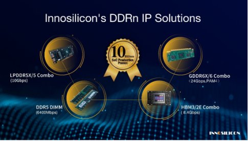
Innosilicon has a full range of high-end DDR IP solutions, including upcoming GDDR7, GDDR6X/6, HBM3/2E, LPDDR5/5X, DDR5/4, LPDDR4/4X/3, DDR4/3/3L, LPDDR3/2, DDR3/3L/2, PSRAM/ONFI/SDIO/EMMC/RPC and other series of IP. Fully support JEDEC standards, including physical layer and controller IP, PPA leading at least 20%, fully covering the world's major foundries 55nm to 3nm process nodes, has been in a large number of customers mass production verification, can be called the ceiling of the DDR IP industry.
Thanks to more than ten years of core technology precipitation and mass production experience in the field of high-speed interfaces, as well as a deep understanding and forward-looking insight into DDR technology, Innosilicon Technology continues to polish its strength, has the high-end DDR IP with the most complete interface types and process coverage, and provides a full-stack solution with high performance and cost advantages, empowering global developers and design enterprises. The solution has launched mature products on each DDR advanced standard, and a number of blockbuster commercial IPs have achieved the industry's only and industry-leading: when the industry's highest rate standard LPDDR5X is still 8533Mbps, Innosilicon already has mass-produced LPDDR5/5X Combo IP with a rate of more than 10Gbps with advanced technology; its latest GDDR technology is GDDR6/6X Combo IP (PAM4) GDDR6 speed up to 18Gbps, GDDR6X rate up to 24Gbps, future-oriented GDDR7 has also entered the research stage; HBM3/2E Combo IP operating rate has reached 8.4Gbps.
In view of the technical difficulties faced by DDR development, such as data crosstalk, phase alignment, signal acquisition, and clock architecture, Innosilicon DDR IP uses a large number of high-performance IO interface technology, anti-noise and signal equalization recovery technology to provide reliable SI/PI analysis and Training, support higher bandwidth per pin, lower working voltage, and have the characteristics of low latency, small size, and scalable design, which can adapt to more application scenarios and be compatible with more DRAM protocols. Reserve a channel for newer DRAM technologies, providing low-cost and flexible scalability for high-end product systems.
Innosilicon's full set of high-end DDR solutions provide cross-design, cross-process and cross-package full custom design solutions, Controller and PHY one-stop rapid integration, PPA optimization and customization, support various design automation processes, complete system signal and power integrity analysis, support customized hard core and various package PCB SI/PI full set of solutions, high efficiency and low risk integration services, various application scenarios in one step. This will greatly promote the performance breakthrough of SoCs, empower a wide range of enterprise applications such as cloud, Internet of Things, high-performance servers and workstations, data centers, and help customers extend product cycles, increase application coverage, and improve the market competitiveness of products.
Innosilicon's high-bandwidth DDR series solutions are industry-leading and all-in-one DDR IP houses
The world's only HBM3/2E Combo IP product
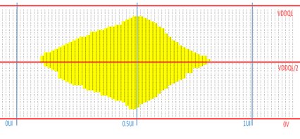
HBM3 transmission rate up to 8.4Gbps, memory bandwidth 920GB/s, HBM2E transmission rate 3.6Gbps, memory bandwidth 460GB/s, support 2, 4, 8 or 12 DRAM stack height, single layer maximum capacity can reach 24G; support ECC, DBI/DM, support AXI, OCP or local user logical interface, as well as data tuning repair and various modes of automatic training
(the figure below is 6.4Gbps HBM3 test electronic eye diagram)
The world's only GDDR6X/6 Combo IP product with a rate of up to 24Gbps
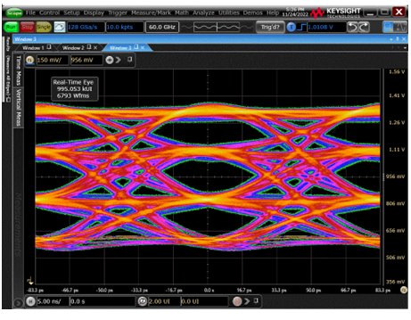
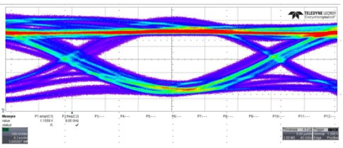
GDDR6/6X Combo IP adopts single-ended PAM4 technology, a single DQ can reach an ultra-high rate of 24Gbps, the system bandwidth exceeds 5Tb/s at 256-bit width, providing a maximum bandwidth of up to 84G/s, supporting quadruple data rate (QDR) and double data rate (DDR) data (WCK) Mode
(24Gbps GDDR6X PAM4 test electronic eye diagram and 18Gbps GDDR6 test electronic eye diagram below)
The world's fastest LPDDR5X/5, breaking through the limit, with a rate of up to 10Gbps
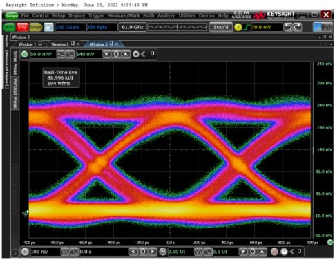
LPDDR5X realizes the access rate of memory particles over 10Gbps over long distances on ordinary PCBs, covering the technical development route of memory particle manufacturers in the next few years; LPDDR5 reaches 6.4Gbps; supports up to 15 training modes, supports multi-rank, supports multiple low-power modes; x16/x32/ x64 data path interface expandable
(10Gbps LPDDR5X test electron eye diagram below)
The world's fastest and most energy-efficient DDR5 with speeds up to 6400Mbps
DDR5 supports up to 6400Mbps, DDR4 reaches 3200Mbps; supports DDR5 and DDR4 LRDIMM, RDIMM, UDIMM; x16/x32/x64/x72/x80 The data path interface is expandable, supporting x4, x8, x16 device types; PHY independently supports a variety of automatic training and DFE, FFE and other signal enhancement technologies
DDR4/3/3L/LPDDR4/4X/3 Combo IP
LPDDR4/4X supports up to 4266Mbps, DDR4 reaches 3200Mbps, DDR3/3L reaches 2133Mbps, LPDDR3 reaches 1600Mbps; supports multi-rank, supports multi-frequency point fast frequency cutting; DDR4 and LPDDR4 support up to 2400Mbps in Wirebond package; x16/x32 data path interface can be expanded
DDR3/3L/2/LPDDR3/2 Combo IP
DDR3/3L reaches 2133Mbps, DDR2/LPDDR2 is 1333Mbps, LPDDR3 is 1600Mbps; extremely low-cost solution, supports SIP or 2-layer PCB implementation; integrates multiple DFT modes; and the x16/x32/x64 data path interface is scalable
PSRAM/ONFI/SDIO/EMMC/RPC and other DDR custom IPs
Support DDR class IO, PSRAM mode and signal with multiple voltages and speeds, with rates covering 100Mbps to 2400Mbps; x8 data path interface, support DLL, PG, single-ended ID, differential IO, ZQIO, bidirectional IO and other complete IO solutions, support special protocol development and IP implementation, support customized modification of special IO, complete various IO libraries
The person in charge of delivering the GPU of Innosilicon Technology said, "Equipped with DDR independent innovation technology, the GPU series of Innosilicon Fantasy has greatly improved the performance and user experience of domestic graphics GPUs. From DDR5/4/3 to LPDDR5X/5/4 and GDDR6X/6, Innosilicon has also achieved full coverage of DDR series of high-bandwidth IP technologies, providing important technical support for global developers and design enterprises, and empowering global partner product success. ”
"The success of customers is our success!" As a global one-stop high-performance IP and chip customization provider, Innosilicon has been deeply engaged in high-speed interface IP for 17 years, has an experienced R&D team, and is a well-known IP and high-end chip customization service veteran manufacturer in the industry. With continuous investment in R&D, continuous pursuit of innovation and long-term accumulation of underlying technology, Innosilicon is far ahead in the field of high-speed interface IP, with three significant advantages: First, high-end performance, whether DDR, SerDes or Chiplet, excellent performance, comprehensive coverage, to meet the needs of interface products; Second, high-end process verification, mainstream advanced processes have been developed and verified and authorized customers for mass production, including 12nm/ 10nm/ 8nm/7nm/6nm/5nm/ 3nm, is the world's two major 5nm advanced process joint certification of the official technical partner; Third is cross-platform, to ensure production smoothly, Innosilicon has a cumulative tape-out verification experience of more than 200 times, high-end IP authorization of more than billions of mass production applications, to help more than one billion FinFET custom chips successfully entered mass production, to ensure the customer product development 100% success to provide back-up services, can accelerate SoC development and reduce risks, trusted by hundreds of well-known enterprises such as AMD, Microsoft, Amazon, Qualcomm, AXAM.
Based on rich IP achievements, as well as more than ten years of advanced process customization experience and global supply chain capabilities, Innosilicon has also formed a full set of chip customization mass production services covering system architecture, bus/core integration, IP integration/SoC integration, and empowers customers' final products with IP full-stack capabilities and chip customization, truly accelerating the whole process and minimizing risk. Looking to the future, with the continuous improvement of the demand for ultra-large-scale chip design such as SoC, the value of IP and its multiplexing technology will become more prominent, as the world's leading high-speed interface IP company, Innosilicon's industry-leading high-end DDR IP solutions will empower global customers to achieve extraordinary results.
