by Jürgen Pintaske
CMOS is, and will continue to be, the work-horse process technology of the semi-conductor industry. But designers of large devices, of complex SoCs and of devices using multiple IP elements are finding new families of problems, with long clock chains, device power consumption and the limits of design, verification and test tools.
One major reason for this is that the entire device is normally designed as a single synchronous circuit. By using asynchronous logic many of these problems can be resolved.
The problems
System-on-chip designs try to put more and more functionality on the same piece of silicon, which leads to increased gate counts and longer development times. The mask cost for manufacturing the silicon is increasing exponentially and the minimum production lot of an ASIC has to justify the production overhead. With increasing complexity and tight schedules, a redesign will not only increase cost but waiting for new samples will add 2 to 6 months to the design cycle.
One way to shorten development time is by using IP, ready-made by third parties to be included in the design. This saves time but adds risk as the internals of this function are not fully known.
Many ICs and ASICs are used in mobile applications where the battery should last as long as possible - contradictory to higher current consumption at higher clock frequencies. Battery voltage varies considerably, depending on load status but since complex designs require very tight supply voltages, a high percentage of the energy is merely consumed in the voltage regulator and generates heat.
But even the basics of the design are beginning to cause problems. Higher clock frequencies draw higher current, and power is only kept under control by using lower voltages.
High clock frequencies and long clock lines can run into EMI effects, with the clock-line acting as an antenna. Powering down areas not in active use reduces power consumption, but adds to design complexity.
Design verification and test tools all have to deal with the entire device as a single synchronous unit, increasing the tool complexity and extending the time taken for tasks like synthesis or simulation.
Asynchronous Logic
Asynchronous logic is not new: it was discussed 20 years ago but with some exceptions it is still in the research state. Engineers have, until now, hesitated to use it as there are not many tools available. EDA tools are designed to implement synchronous functionality and this has lead to the steep increase in on-chip functionality. If all signals generated on-chip switch at the same time, the verification of the system is simplified: it has "only" to be verified that the delays from the output of the registers via the combinatorial logic are shorter than the next clock. This can be viewed as "pure work" compared to a system built in asynchronous logic where the external asynchronous behaviour has to be understood more clearly. But synchronous and asynchronous logic are not exclusive: a synchronous implementation is a special case in the space of all the asynchronous design possibilities.
Let us take a well known example: soldiers marching over a bridge. If they march in lockstep there is the danger of vibration, if they march out of step the problem disappears. This analogy can explain the different noise/EMI behaviours; in a synchronous system there are current spikes when the clock switches the registers, with an asynchronous implementation these values are reduced by 10 dB.
The SOC - a big state machine
How does a system work as synchronous design and how can we change this to asynchronous? In a synchronous system all the inputs and outputs are synchronized to the clock. The whole chip acts like a big state machine (Figure 1a). It consists of two blocks: one for the Boolean logic without feedback and one for the registers which latch the actual status when the clock signal rises. The status is fed back as part of the logic inputs. When the clock signal rises, the current status is "frozen". The signals at the outputs of the logic have to have stabilized before the next clock, which means that the clock period has to be longer that the longest "critical" path through the logic. On the other hand the clock frequency has to be high enough, to catch all the input changes (Figure 1b). All signals on-chip are forced into lock-step by the clock, which achieves a clear signal relationship for design, verification and test.
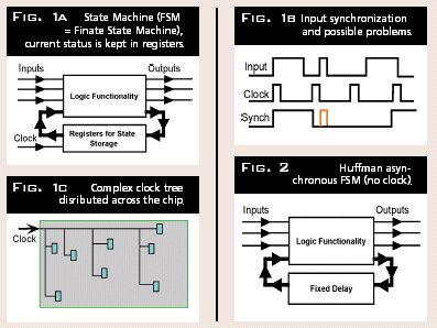
If all these gates are located close together there is no problem. In a real system (figure 1c) the registers are distributed across the chip sometimes consisting of millions of gates. The longest and most critical path then is the clock network needing many additional buffers to keep sharp clock edges but at the same time causing delays and power consumption. At high clock rates the long clock lines act like antenna, causing EMI. Both effects are, unfortunately, happening even if there is no activity on the inputs or outputs.
In the past and with older technologies, the issues were different: wider metal traces caused less delay than the gates that did the processing, so the clock problem was less of an issue. Modern silicon technologies use very narrow traces for connections and the speed of gates has increased. On the same silicon area the number of gates has increased dramatically and the clock line has such length and complexity that synchronising all registers on chip gets increasingly difficult.
No clock line
In an asynchronous design this clock line connecting all the registers does not exist. All the functions still have to be co-ordinated but in a different way. One way to describe it is to subdivide asynchronous systems into three groups with different requirements: small, medium and large.
Some aspects of asynchronous design are described in table 1. There are signals, transfer of data and propagation of signals on the chip. Boolean algebra only describes the logic behaviour but does not take delays in the wires or the gates, dependencies of supply voltage, temperature, and length of connections or process variations into account.
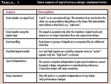
Signals in digital chips can only take the levels high or low.A slow transition will cause a delay until the next gate switches. It would be easier to act on the change of level rather than on the level.
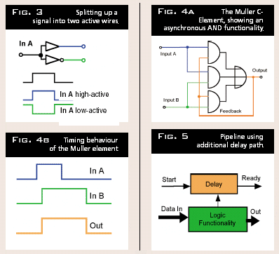
One alternative is to define different lines to carry the high and the low signal (Figure 3). This will increase the wiring on-chip but now there are only active signals and only one of the two signals can be active at the same time. If many parallel lines have to be routed on the IC then bundling is a possibility with the signal lines and the related clock are running next to each other, retaining the relative relationship. The aim is to develop the system as speed independent and completely delay insensitive.
The most common technique in asynchronous design uses dual-rail signals and level sensitive signal coding. Systems built in such a way are delay insensitive and supply voltage, temperature and process variations will not influence functionality: only throughput is affected.
Small asynchronous systems or functions
Control functions are a good example for such an implementation. Complexity is limited and the complete functionality can be described. In figure 1 the diagram of a state machine was shown. If the design only allows one input signal to change at a time ( for example the 10 keys of a keyboard with priority encoding or in Gray code) and all signals have stabilized before the next change then a Huffman FSM without clock can be used. Here the delay takes the function of a clock (Figure 4b).
Dual-Rail encoding
One other possibility would be to design with active signals only. Often it is forgotten, that high is not the only signal: low is a second signal. If we divide high and low onto two different rails then the active signal is automatically coupled with the related clock signal (Figure 3). From now on only the "high" states are important and a low means "inactive" so every signal carries its own clock signal. If there are no changes then no gate switches and there is only quiescent current. The gates for such an implementation have to work differently now: only high inputs can change the output. And all the signals have to be present and active. If one wire is broken the gate cannot change the output anymore.
One example would be voting: there is a yes vote or a no vote. Both together are not allowed. Such a type of logic need not be used only at gate level. Theseus owns a patented asynchronous logic implementation, which it offers as licenses and uses it to design asynchronous systems, IP and micro-controllers. NCL (Null Convention Logic) uses a special type of implementation where all the active signals first fire to generate all the outputs. Then a so called NULL cycle is executed to reset all internal feedbacks followed by a new active cycle.
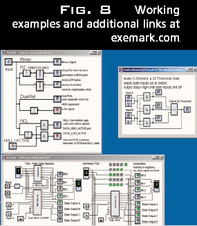
The Muller C-Element (Figure 4) shows the functionality of such an asynchronous gate. The additional feedback loop generates a special sequential behaviour. With both inputs inactive the output is low (inactive). The first (faster) input does not change the output, this happens when the second input also becomes active. If one input changes to inactive the output stays active via the feedback. When the second input becomes inactive the output switches back to inactive (low).
The data path in medium complex systems
Systems with medium complexity have buses as well as the control structures. They also have to have cater for correct hand over. The different functional blocks on a chip can transfer data only when additional signals indicate that the data is stable and can be latched (Figure 5). This can be achieved by adding a "Start" signal which triggers a fixed delay longer than the critical path in the related logic section. The "Ready" signal will indicate that the output signals have stabilized. In such a setup none of the gates work at maximum speed as the safety factor in the parallel delay chain will define the maximum throughput.
Data transfer using "Handshake" signal
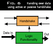
It would be better if neighbours co-operate and in the passive version the sender indicates that data is available. The next block in the chain accepts the data and indicates to the sender via "Ready" that another word can be prepared and a new cycle can start (Figure 6). Data and handshake propagate in the same direction. The active version works different. Now the receiver indicates that he is waiting for data.The delivery is indicated by the sender. Here data and request propagate in opposite directions.
Micro-Pipelines
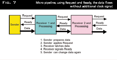
If we combine the computation of data using the parallel delay and the Request/Ready sequence we achieve a very efficient way of communication between asynchronous blocks (Figure 7). A similar way of data communication has been used in the development of the various Amulet processors based on the ARM architecture. To co-ordinate various delays onchip, FIFOs (first-in, first-out) and LIFOs (last-in, first-out) are implemented to make sure that the data arriving asynchronously is available at the right time for further use.
Hardware und Software
The problem of asynchronous data processing is not only existing for hardware. Exactly the same problems will be present in a system with parallel processing running on multiple processors or when processing parallel processes on a single processor if the data to be worked on is not synchronized. It both cases the data has to be stable and unchanged for the next task. Other areas where this was relevant was in Petri Nets, or in communicating sequential processes (CSP) and a couple of years back in Transputers, where the communication between multiple transputers was based on CSP.
The buzzword “hardware- software codesign†pops up more and more as the simulation of complete systems is increasingly used. Simulation in C is independent of any later implementation, so it is undefined if the different functionalities are implemented in hardware - meaning gates - or in software - a program running on a microprocessor. The decision will be taken later, based on issues like speed of execution, cost of hardware, volume of production, processor used and so on. This leads to decisions if the implementation will be able to react to fast asynchronous events or if the maximum throughput is defined via the microprocessor.
Implementation
In such a system the software will be optimised by the C-Compiler and the hardware by logic synthesis. If asynchronous reaction is needed this does not necessarily mean that the use of standard tools is excluded. Table 2 shows some examples of transistor counts in implementations as synchronous logic or as asynchronous logic in NCL technology. The ratio of these examples is between 0.7 and 2.1. This does not take into account how much space, complexity and transistors on the chip are saved by using asynchronous NCL. It is important to trade off higher gate counts and faster development times.
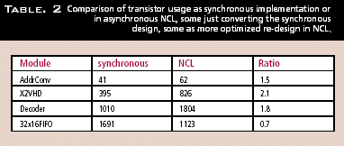
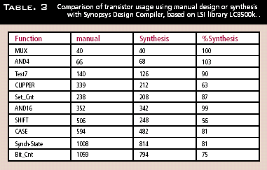
Table 3 shows an indication of how a manual design compares to the use of the Synopsys Design Compiler.
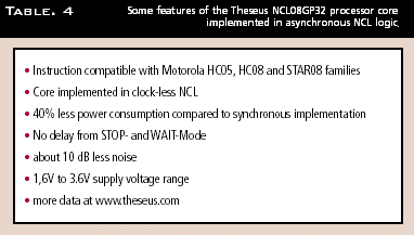
The best indication for a real comparison is the implementation of the NCL08GP32 (Table 4), a microcontroller instruction compatible with the Motorola HC05/HC08/STAR08 families.
Summary
Asynchronous logic - yes or no?? This will probably be the wrong question in the future.As clock rates and gate counts increase to achieve more functionality, designers of mobile consumer products will be forced to look at new ways to save power. It is possible to switch off unused functionality in synchronous designs but this has to be paid for by additional hard or software. Another buzz word in this context is IP. The main problem of intellectual property is the reliable co-operation with other blocks on the same chip. In a synchronous design the clock frequency has to be right for all the blocks on the SoC. Changing this to an asynchronous interface would decouple them and each block could function independently. The measure would be minimum throughput, which could lead to important savings in time and cost of design.
The better question will be: how much asynchronous functionality on-chip and when and why. Already now there are asynchronous implementations of microcontroller products and IP available. These are instruction compatible with some Motorola families, and use the NCL technology developed by Theseus. This is based on industry standard tools like Design Compiler from Synopsys. Products using asynchronous technologies from other suppliers are under development.
Asynchronous technology promises to be an important tool in the toolbox of designers working on large and complex devices.
