By Supriya Unnikrishnan and Sujith Mathew Iype (Ignitarium Technology Solutions)
With the tremendous increase in the intelligence added to various consumer and professional devices, the applications are turning more data-centric and computation intensive. From the IC design perspective, this enhances the already existing challenge of power vs area trade-off. Power Analysis is not a new terminology in the semiconductor design cycle. But there is a difference in opinion regarding the most efficient phase of the design cycle for power analysis. An architecture phase will be too early, and physical design phase will be too late for the power estimation. Of late, there is a tendency to analyze power hot spots during the RTL phase of the project. RTL based power analysis is faster and easier to perform and has a shorter iteration time than the analysis at later stages. This article addresses some of the power optimization techniques applied at the RTL level.
A radical increase in battery-driven consumer appliances made power optimization an essential feature in most systems on chips (SoC). In the early phases of the VLSI industry, power analysis was considered a back-end activity where the front-end design interactions and contributions were minimal.
But as the chip complexity increases, with different power and voltage domains, it became mandatory to move power analysis to the front-end phase to ensure proper estimation and optimization. The power figures are so competitive that optimization only at the back-end phase falls short of the requirement. Also, the dynamic power calculation depends very much on the input vector driven to the SoC; hence, analysis with functional verification vector input appears mandatory. Thus, the industry started doing power analysis at the RTL phase.
There is scope for power optimization at different stages of ASIC design. System partitioning into power and voltage domains is done at the architecture phase. Defining power modes like active and hibernation allows optimization even with a single voltage domain. Power gating the circuitry except for wake-up logic while the processor is in hibernation mode reduces power wastage. These are some of the conventional approaches applied for power reduction. In multi-core processor designs, multiple voltage domains allow the supply voltage to each core to be controlled based on the workload. A core operating at higher voltage operates at a higher frequency, whereas a core applied with lower voltage can use lower frequency. The memory organization and module level clock gating is another area where architecture level optimization is applied.
Power reduction during the synthesis phase owes to gate transistor sizing and cell merging to reduce net switching activity. Another approach is to assign a high switching net to a pin with lower capacitance and a low switching net to a logically symmetric pin with higher capacitance. Synthesis tools enable clock gate insertion by converting data enables to clock-enable. Design optimization over leakage power by mapping non-critical paths and critical paths in the design by cells with different threshold voltages is another technique applied at back-end. The power optimization at RTL level mainly focus on reducing signal activity at the register level. This article primarily focuses on RTL optimization, which captures power control at a more granular level.
II. POWER AWARE RTL
In general, exploring RTL power optimization includes close monitoring of the following aspects of the design.
- Clock gating at register level to reduce switching
- Finite State Machine(FSM) based control on gating downstream or upstream logic path
- Gating data path operator input when not enabled
- Reducing redundant activity in the combinational circuit
This section addresses some optimization techniques, citing user scenarios and coding examples.
A. Clock Gating
Clock gate insertion at the block level is a prevalent method to reduce power. But clock gate insertion at the register level is employed only when power constraints are so stringent. This is due to the area cost inferred from the clock gate insertion at a granular level.
To enable clock gate insertion at the register level, RTL is written in such a manner that the synthesis tool automatically inserts clock gate. Another option is to manually configure synthesis tools to insert clock gate for selected registers. In a complex design, the second option is not feasible. In such a scenario, RTL is written in a way so that tool infers the clock gate from code.
Consider the generation of fifo wr err signal asserted when FIFO is full and write is launched. The example code listing 1 doesn’t infer clock gate, whereas listing 2 infers clock gate.
Listing 1. Code without CG Inference
always @(posedge clk or negedge reset)
if (reset = 0)
fifo_wr_err <= 0
else
fifo_wr_err <= fifo_full & fifo_wr_en ;
The code listing 2 will infer a clock gate with enable as fifo wr en. This will get toggled only when fifo wr en is there .
Listing 2. Code with CG Insertion
always @(posedge clk or negedge reset)
if (reset = 0)
fifo_wr_err <= 0
else
if (fifo_wr_en)
fifo_wr_err <= fifo_full;
1) Clock Gating Efficiency: Insertion of clock gate without investigation on clock gating efficiency may increase power figures. The following factors estimate clock gating efficiency
- All bits in a bus are being clock gated
- The percentage of total clock cycles which are gated
- The data toggling at the enabled clock cycles
The listing 3 shows an example of efficient clock gating, which is enabled only when input at the register changes.
Listing 3. Improved Clock Gating Efficiency
always @(posedge clk or negedge reset)
if (reset = 0)
fifo_wr_err <= 0
else
if (value_en)
fifo_wr_err <= nxt_fifo_wr_err;
assign nxt_fifo_wr_err = fifo_full & fifo_wr_en;
assign value_en = fifo_wr_err ˆ nxt_fifo_wr_err;
2) Clock Gating TradeOff: When we strive for 100 percent clock gating efficiency, the system’s area figures will increase drastically due to using clock gates specific to each register. To avoid this, we can follow trade-off where we use weak enable for clock gating. Here, we combine the enables for multiple registers even though there will be redundant toggling at flip flop inputs. The recommendation for the default value of this trade-off is 3-4, which means a common enable is shared across 3-4 registers at the expense of reduced clock gate efficiency.
The listing 4 and 5 shows how this can be implemented for the FIFO example. The write error and read error generation enable can be combined to reduce area cost.
Listing 4. Combined Clock Gating Example 1
always @(posedge clk or negedge reset)
if (reset = 0)
fifo_wr_err <= 0
else
if (value_en)
fifo_wr_err <= nxt_fifo_wr_err;
assign nxt_fifo_wr_err = fifo_full & fifo_wr_en;
assign value1_en = fifo_wr_err ˆ nxt_fifo_wr_err;
always @(posedge clk or negedge reset)
if (reset = 0)
fifo_rd_err <= 0
else
if (value_en)
fifo_rd_err <= nxt_ fifo_rd_err;
assign nxt_fifo_rd_err = fifo_empty & fifo_rd_en;
assign value_en = fifo_wr_err ˆ nxt_fifo_wr_err | fifo_rd_err ˆ nxt_fifo_rd_err;
Listing 5. Combined Clock Gating Example 2
always @(posedge clk or negedge reset)
if (reset = 0)
fifo_wr_err <= 0
else
if (fifo_en)
fifo_wr_err <= nxt_fifo_wr_err;
always @(posedge clk or negedge reset)
if (reset = 0)
fifo_rd_err <= 0
else
if (fifo_en)
fifo_rd_err <= nxt_fifo_rd_err;
assign nxt_fifo_wr_err = fifo_full & fifo_wr_en;
assign nxt_fifo_rd_err = fifo_empty & fifo_rd_en;
assign fifo_en = fifo_wr_en | fifo_rd_en;
B. FSM based Control
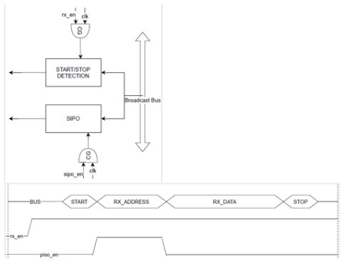
Fig. 1. FSM Based Enable Generation
Based on the design, FSM-based control signals is used to gate downstream or upstream paths.
Example 1 : FSM is used to control the transmit path and receive path of a device that is enabled either in transmit or in receive mode. The signals generated based on the FSM state can be used to gate all logic for transmission and reception.
List 6 shows how the enables are generated based on the FSM control.
Listing 6. Enable Generation based on FSM
assign transmit_cg_en = ˜state_tx[IDLE];
assign receive_cg_en = ˜state_rx[IDLE];
Example 2 : In the above scenario, consider the device is plugged into a broadcast serial bus where all devices must listen to the bus for a particular duration. We can gate the external bus transition propagation to internal logic after confirming that the transaction is not addressed to the device once the listening period is over, as shown in figure 1. The start
and stop detection of the bus protocol is constantly active. In contrast, the Serial In Parallel Out (SIPO) logic is active only during a listening period if the transaction is not addressed to the device.
C. Data Path Operator
The data path operator blocks like multipliers can have unnecessary toggling at the input even if these are not enabled.
The following techniques reduce power dissipation due to this.
- Clock gate the sequential logic providing input to the data path operator
- Use a latch at the input to data path operator or gate inputs with the enable
Listings 7 and 8 depict the code to realize this.
Listing 7. Gating Data Operator Input Toggling Method1
always @(posedge clk or negedge reset)
if (reset = 0) begin
mul_in1 <= 0
mul_in2 <= 0
end
else
if (mul_en) begin
mul_in1 <= nxt_mul_in1;
mul_in2 <= nxt_mul_in2;
end
Listing 8. Gating Data Operator Input Method 2
assign mul_in1 = data_in1 &
{DATA_WIDTH{mul_en}};
assign mul_in2 = data_in2 &
{DATA_WIDTH{mul_en}};
Listing 9. Gating Data Operator Input Methos 3
always@(mul_en) begin
if(mul_en) begin
mul_in1 = data_in1;
mul_in2 = data_in2;
end
end
D. Reducing activity at Combinational Logic
The power dissipation at the combinational logic can be controlled by avoiding unnecessary toggling at the inputs. A multiplexer can be considered here as example which is the major building block of the combinational logic.
In the example circuit given in figure 2, we have a shared data memory accessed by two packetizers. Here we do have the apparent power wastage since the input to packetizer 2 will toggle when packetizer 1 is accessing data and vice-versa.
A more power optimized design will gate input to MUX in packetizer 1 when packetizer 2 is accessing data memory as shown in figure 3
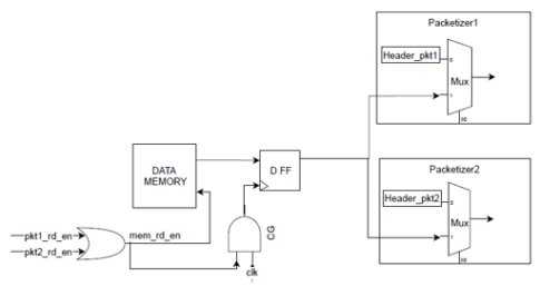
Fig. 2. Toggling at Mux Input
In the above example, if we can split the memory into small words, we can gate memory block and result in more effective power gating. But the disadvantage will be in routing congestion and duplicating the DFT logic for memories.
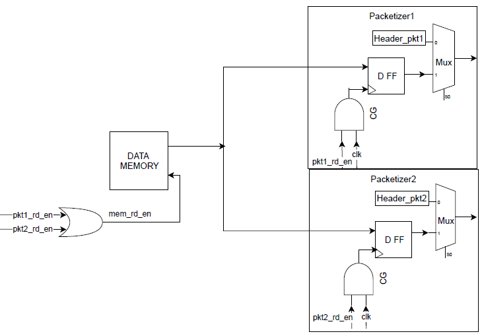
Fig. 3. Gated Toggling at Mux Input
III. RTL POWER ANALYSIS TOOLS
The ASIC design flow is getting updated with RTL analysis tools that account for power analysis and reduction at an early stage so that power budgeting is complete as early as possible. Joules RTL power solution from Cadence and PowerArtist from Ansys are such tools that does Power Analysis and Power Reduction early in the design cycle.
The RTL power analysis tool flow is shown in figure 4.
RTL design files are elaborated and analyzed for clock and data activity using simulation activity files given in VCD, SAIF or FSDB format. The input to the power estimation
stage includes a library with power information, including Vt-based classification, capacitance estimation based on wire load and spef model, and clock definition. The clock definition information includes SDC file of the design, the definition of clock gating cell and minimum bit width for clock gating, and clock buffers to be used for root, branch, and leaf node.
The power analysis results are reported as two categories [2] [3] ‘Power Reduction’ look at the implementation and will try to analyze power saving, power penalty, and area impact for a different implementation technique. ‘Power Linter ’ recommend a means of recovering the wasted power, as the method of recovering depends heavily on the design and test pattern.
A. Power Reduction
By default, the synthesis tool uses locally available enables to clock gate register banks. This is useful but not enough to address complex designs. The clock gating based on logic observability analysis generates new enables from downstream
or upstream logic. There are situations where, in a design, the output of register (or output of downstream logic) is not used (not observable) downstream. These situations are used to clock gate the register.
B. Power Linters
Power Linters identify power spots by doing analysis based on a RTL checklist. The tool can be configured for examining RTL for many guidelines including
- Data should not toggle when clock is in-active
- Memory Bus should not toggle when write control is disabled
- No activity should be observed when a Mux line is not selected
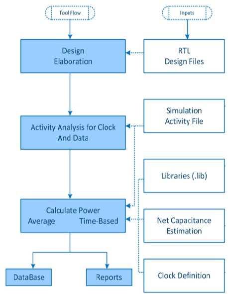
Fig. 4. RTL Power Analysis
IV. EXPERIMENTAL ANALYSIS
A representative design as shown in fig 6 is used for the experimental analysis. The design captures representation of the various circuit components discussed in section II. RTL is developed for the design by incrementally enabling different power optimization techniques discussed in the section. RTL power analysis tool Joules from Cadence is used for the analysis.
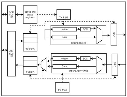
Fig. 5. Block Diagram
Experimental studies are conducted in two phases.
- Initial analysis is performed using RTL not optimized for power. Tool configuration is explored here, to derive the optimal tool set up.
- RTL adhered to power guidelines is used for analysis to understand the incremental improvement obtained in power metric.
Phase 1 study presents the clock gate(CG) inference by tool based on the vector activity analysis. The user scenarios are simulated with different toggling rate for generating vector activity database. If CG inference is enabled, additional clock gating opportunities are explored by tool even in the absence of mux feedback into the register. The power value reported by the tool is captured in Figure 6. The CG min and CG max values indicates minimum and maximum number of flops that can be driven by a CG cell.
Even if RTL is written without multiplexer feedback into the register used to infer CG, tool will insert clock gating cells at global points. In the design under consideration, tool
inserts clock gating at the following points when CG inference is enabled.
- Gating based on the APB slave interface FSM. Since register write won’t happen unless register access is selected by external APB interface, tool gates the clock to register module based on the APB FSM logic. Whenever select is high, the clock to register modules are ungated.
- Similarly TXFIFO and RXFIFO logic is gated based on the axi slv if logic. The clock is ungated only when the AXI interface is active.
The trade-off between power saving and area overhead is presented with the help of FoM (Figure of Merit) defined as multiplied value of Power and Area ( PowerxArea). The optimal min-max value ideal for system is identified
through this analysis, for a constant system frequency and switching activity. In some cases, top down approach can be applied where a top level min/max is defined and this value is overwritten in the sub block. As observable from the figure, there is an optimal CGmin and CGmax value beyond which there is no improvement in the FoM.
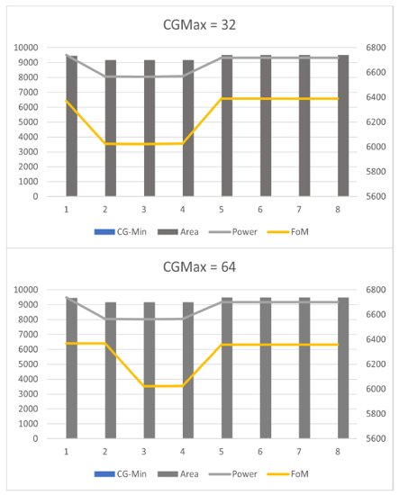
Fig. 6. Analysis of CG insertion by tool
In the second phase of the experimental studies, power optimized RTL is provided as input to the tool as described below.
1) The incremental changes for optimization are made in RTL as per the guidelines captured in section II
- The clock gating efficiency of the counters, FSM registers etc. are increased by modifying enable logic.
- FSM Based control is used to ensure that Transmit and receive related flops are enabled only when FSM is in transmit and receive state.
2) Combinational activity is reduced following guidelines in section II C and D.
3) Optimization is done based on the use case of the system and the metrics under consideration. Inefficient enable can explode area without improvement in power values. Examples of some optimization techniques applied are cited below.
- In the register module, a high level gating is inserted by tool based on the control signal from AXI FSM. But even with this, clock to every register toggles every time there is an access initiated to register space. To avoid this, configuration space is split into two register space and second level of reg sel is used for these sub-blocks. The division is based on the frequency of access by host. One-time configured register group can improve clock gating efficiency at lesser area cost.
- For frequently written registers, clock gating efficiency is maximum when enable is generated whenever there is a change in register value. But this will add to the area. As a trade off, we can use this enable only for portion of register. For example, there is a control register which has 8 bit field which give packet length which is written with the same value as per the use case. In that case, instead of generating enable for whole 32 bit register, we can generate enable only for the lowest 8 bit of register which is almost every time written with same value.
assign enable = reg_bus[7:0]
ˆ nxt_reg_bus[7:0];
assign enable = reg_bus[31:0]
ˆ nxt_reg_bus[31:0];
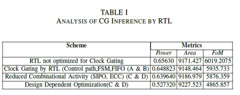
ANALYSIS OF CG INFERENCE BY RTL
In addition to these, we can use tool reports to get more inputs on the different power hot spots. Observability Don’t Care (ODC) is one such technique to derive new clock gate enables based on analysis of downstream logic for observability of register output. There are situations where, in a design, the
output of register (or output of downstream logic) is not used (not observable) in the downstream [2]. The report odc report the wasted ODC power and suggestion for enable generation. Along with the analysis based on the system use case, these techniques can be effectively clubbed to generate a power optimal design.
V. SUMMARY
The target power metrics for low-power chips demand power optimization to be enabled in all stages of the chip design. A simple change in RTL can save a lot of dynamic power and further reduce the time and effort spent in later stages of design to achieve optimal values. For a low-power design, RTL developed by adhering to the power optimization guidelines significantly contributes to the early closure of power budgeting.
REFERENCES
[1] Early Power Closure Using a Design for Power Methodology: Ansys White paper
[2] Power Artist Reference Manual Software Release 2019 R2.5
[3] Joules User Guide for Legacy UI
