By Samir Shaikh and Vimal Gohel (eInfochips)
Abstract:
The relentless march towards shrinking technology nodes has ushered in a new era of intricate semiconductor designs characterized by a proliferation of transistors. This intensifying complexity brings with it heightened criticality in various aspects of chip design and manufacturing. As each day dawns, innovative techniques and methodologies emerge to tackle these burgeoning challenges and fortify the compatibility of cutting-edge electronic devices.
Keywords — ASIC, Placement, Useful skew, CTS - (Clock tree synthesis), Soc- system on chip
Introduction
In the relentless pursuit of faster and more efficient integrated circuits, the semiconductor industry has embarked on a remarkable journey, venturing into the incredibly small 5nm technology node. At this scale, the stakes are higher than ever, and every nanosecond counts. The key to unlocking the full potential of 5nm technology lies in optimizing one critical aspect: timing.
This research delves into the strategies and techniques that engineers and designers employ to improve timing at the 5nm technology node. We will explore the art of useful skew in this article. Together, this method forms a comprehensive toolkit for meeting the demands of modern computing, enabling faster, more energy-efficient, and higher-performing integrated circuits.
On this journey, as we navigate the cutting-edge world of 5nm technology, even the slightest adjustments in design can make a world of difference in the race against time. The future of computing depends on it, and it all begins with understanding the intricacies of timing optimization.
Design area and meeting timing goals can be achieved by increasing cell density in less crowded locations. To maximize cell placement and reduce congestion, strategies like placement blockage are used.
What is skew
Clock skew is a phenomenon where the clock signal that is used to synchronize the operation of different components within an integrated circuit arrives at different parts of the chip at slightly different times [4].
Consider a synchronous digital circuit with a clock signal that drives multiple flip-flops. In an ideal scenario, all flip-flops would receive the clock signal simultaneously, ensuring synchronized behavior. However, due to various factors such as differences in wire lengths, variations in transistor characteristics, or process variations, the arrival times of the clock signal at different flip-flops may vary.
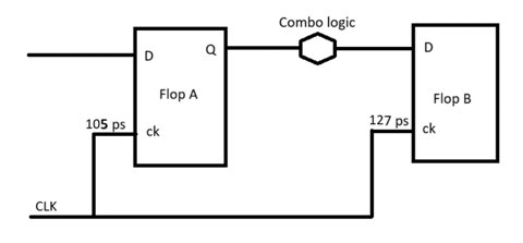
Fig.1 Clock signal arrives simultaneously at Flip-Flop A and Flip-Flop B.
Both flip-flops capture their input data at the exact rising edge of the clock. This scenario ensures proper synchronization, and there is no skew between the clock arrival times at the flip-flops in an ideal world.
Equation for skew
S = t2 – t1
Where: S is skew, t1​ is the arrival time of the signal at the first point and t2​ is the arrival time of the same signal at the second point.
Due to variations in the physical characteristics of the circuit, the clock signal reaches Flip-Flop A later than Flip-Flop B. The time difference between the clock arrival at Flip-Flop A and the arrival time at Flip-Flop B is the skew. If this skew becomes significant, it can lead to either setup or hold timing issues.
Assume there's a setup time requirement for both flip-flops, specifying the minimum time the input data must be stable before the rising edge of the clock. If the skew is such that Flip-Flop B receives the clock significantly later than Flip-Flop A, it might lead to a setup time violation for Flip-Flop B. Flip-Flop A might meet its setup time, but the data at Flip-Flop B might not be stable long enough before its clock edge, causing potential errors.
A. What is useful skew
Useful skew in a synchronous digital circuit refers to the timing of the design [1]. This intentional manipulation of timing is purposeful and controlled adjustment of signal arrival is strategically employed to address specific timing requirements. Deliberately adjusting the timing of signals, useful skew can be used to optimize critical paths within the circuit.
The primary objectives of introducing useful skew include mitigating issues like setup and hold time violations. Setup time violations occur when the data signal arrives late. Hold time violations occur when data signal arrives early. This deliberate adjustment not only helps in achieving synchronization but also contributes to overall performance optimization, promoting reliable and efficient operation of the synchronous digital circuit.
B. Theoretical test case
Let's delve into a more technical example of useful skew in the context of resolving setup violations:
Consider a synchronous design with three sequential elements, labeled as Register 1, Register 2, and Register 3, all driven by the same clock signal (CLK). However, due to various factors, the arrival times and setup margins for these registers are not ideal [2].
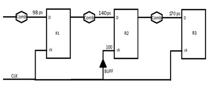
Fig. 2: Synchronous design with 3 Registers
Let's examine the scenario:
Registers and Slack:
Register 1 has a setup slack of 98 ps. Register 1 has a positive setup slack of 2 ps.
Register 2, however, has a setup slack of 140 ps, indicating a setup violation (clock arrives 100 ps after it is required).
Setup slack = required time(clk) – arrival time(data)
On Register 2, the clock arrives earlier (100ps) than the data (140ps), so overall violation is – 40 ps on Register 2. Traditional methods such as adding buffers, upsize cell, vt swapping, and many more can be used to speed up the data path, but we don’t want to apply any traditional method on the data path.[4] The only viable option is to explore clock skew to address the setup violation in Register 2.
Intentionally adding delay buffers in the clock path after CLK for Register 1 introduces skew. This skew selectively impacts on the clock signal reaching Register 2, effectively extending the setup time for Register 2. The delay introduced in the clock path for Register 2 also affects the data path connected to Register 3. Overall, the delay is moved to Register 3. At Register 3, we have enough margin of 170 ps. Useful skew can push that -40 margin to Register 3 using buffer, so at the end, the positive margin is 130ps. If Register 3 has sufficient setup margin to accommodate the additional delay introduced by the skew, it can still meet its setup time requirements. This is how useful skew works.
Practical Approach
In the complex world of digital design projects, a live project encounters a stubborn challenge register-to-register (reg2reg) violations with slack of 61 ps. Let us understand this violation in detail.
Path Analysis with report_timing: Seeking insights, turns to report_timing for a closer examination of the critical paths. We have checked the margins on previous paths of n-1 and n-2, so if we get a positive margin, we can apply useful skew.
Violated path:
report_timing -from pipe2_reg_165_/Q -to pipe1_reg_165_/D
Slack: -61ps
Previous timing path (N-1):
report_timing -from pipe3_reg_165_/Q -to pipe2_reg_165_/D
Slack: +13ps
Previous yprevious timing path (N-2):
report_timing –from pipe4_reg_165_/Q -to pipe3_reg_165_/D
Slack: +200ps
C. Positive Margin and the Role of Useful Skew
Surprisingly, the second path reveals a positive margin at n-2 stage, indicating potential room for improvement. Let’s use the concept of "useful skew." Leveraging the potential of useful skew, we have explored adjustments to fine-tune timing and improve violated setup slack. This involves careful manipulation of Clock Tree Synthesis (CTS) settings and related constraints.
This helps facilitate optimal timing in your design using `opt_design` and `opt_clock_skew` commands, along with the `opt_useful_skew` attribute. The following instructions guide you through enabling useful skew optimization at different stages of the design flow:
1. Enable Useful Skew Optimization:
To enable useful skew optimization globally, use the following command:
set_db opt_useful_skew true
2. Specify Useful Skew Effort in ccopt Design:
Set the level of effort for useful skew optimization in both Clock Tree Synthesis (CTS) and post-CTS flows:
set_db opt_useful_skew_ccopt standard
3. Enable Useful Skew Before CTS:
Activate useful skew optimization before CTS to identify and adjust sequential elements:
set_db opt_useful_skew_pre_cts
4. Enable Useful Skew After Routing:
Enable useful skew optimization in the post-routing phase for further refinement:
set_db opt_useful_skew_post_route
Results and comparison
In the table below, you can find the result of default run with useful skew.
Table 1: Timing statistics without useful skew
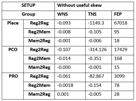
Table 2 Timing Statistic with useful skew
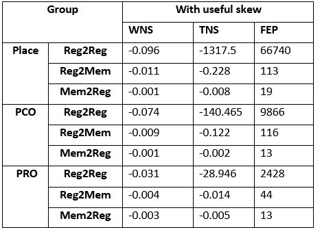
Tables 1 and 2 show the timing statistics with and without useful skew of the design. This contains Worst Negative Slack (WNS), Total Negative Slack (TNS) and Failing End Points (FEP) for all the three path groups at different stages of Place, Post Clock Opt (PCO), and Post route opt (PRO) for setup check. The useful skew is implemented on pre cts stage (place stage) for which all the four steps defined above were enabled in Innovus tool.
Table 3: Hold violation without Useful skew

Table 4: Hold violation with useful skew

Table 5: Design Statistics
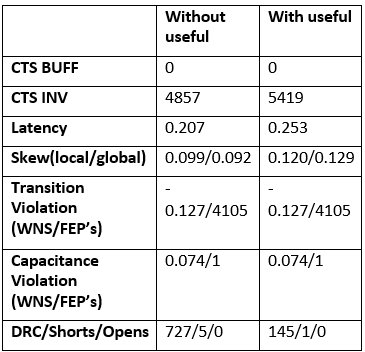
Table 3 and 4 show timing statistics for Hold violations using with and without useful skew, and Table 5 shows the design statistics of the design.
As we observed from the above table, there are merits and demerits of using useful skew in the design.
Merits of Useful Skew:
Useful skews can help meet critical setup and skew can be dynamically adjusted based on the specific needs of different parts of the design or during different operational modes, providing a level of adaptability. In situations where changing the data path is challenging, introducing skew offers a solution that minimizes the need for extensive modifications to the existing design.
Demerits of Useful Skew:
It might worsen hold. Changes in clock skew can have ripple effects throughout the design. The delay introduced in one part of the clock distribution may impact downstream elements, potentially introducing new timing challenges. Introducing skew adds complexity to the design process. Analyze the impact of skew on different aspects carefully such as latency. Using it as a default solution without a thorough understanding of the design's requirements can lead to overcorrection, potentially introducing new timing issues or negatively affecting overall performance.
Conclusion
The understanding and strategic use of clock skew, especially through the application of useful skew, emerge as crucial tools in addressing synchronization challenges. By deliberately adjusting signal arrival times, useful skew not only mitigates setup and hold time violations but also contributes to overall performance optimization. The paper highlighted the practical implementation of useful skew in resolving complex design challenges, showcasing its effectiveness in achieving positive margins and improving overall circuit reliability.
ACKNOWLEDGMENT
We would like to express our sincere thanks to the management of Ganpat university and eInfochips, an arrow company for providing us with the cadence EDA tools. We would like to thank Mr. Nilesh Ranpura (Director Engineering - ASIC at eInfochips Pvt. Ltd, Ahmedabad) for accepting our request and allowing us the usage of these tools to carry out the expected work.
References
- http://www.vlsijunction.com/2015/12/useful-skew.html
- https://vlsi.pro/useful-skew/
- https://vlsi.pro/useful-skew/
- https://chipedge.com/what-is-skew-in-vlsi/
- https://www.vlsi-expert.com/2016/03/types-of-clock-skew.html
- S. Do, S. Kim and S. Kang, "Skew control methodology for useful-skew implementation," 2016 International SoC Design Conference (ISOCC), Jeju, Korea (South), 2016, pp. 221-222, doi: 10.1109/ISOCC.2016.7799867.
- J. Fadnavis and Kariyappa B.S. “PNR flow methodology for congestion optimization using different macro placement strategies of DDR memories.” International Journal of Advanced Technology and Engineering Exploration (2021): 2394-7454.
- Saxena, P., Shelar, R.S. and Sapatnekar, S., 2007. Routing Congestion in VLSI Circuits: Estimation and Optimization. Springer Science & Business Media
- Yifei Sun, Jia Liu, Xin Li, and Xianlong Hong "A Multi-Objective Routing-Driven Placement Algorithm for IR Drop Minimization in VLSI Circuits". It spans across pages 1998-2008 of volume 38, issue 10 of the journal
- Cheng-Chih Huang, Ming-Jie Huang, and Jinn-Shyan Wang. "A Dynamic Voltage Scaling Driven Placement and Routing Flow for IRDrop Reduction in Power Grids" The article is published in volume 35, issue 2 of the journal and spans across pages 201-214.
- https://support.cadence.com/apex/Coveo_CommunitySearch#q=opt_useful_skew&t=AllContent&searchboxDropdown=1&firstQueryCause=searchFromLink&firstQueryMeta={%22expression%22:%22opt_useful_skew%22%20,%20%22advancedExpression%22:%22%22}
- https://support.cadence.com/apex/techpubDocViewerPage?xmlName=tcrcom.xml&title=Innovus+Stylus+Common+UI+Text+Command+Reference+--+opt_clock_skew+-+opt_clock_skew&hash=&c_version=22.13&path=TCRcom%2FTCRcom22.13%2Fopt_clock_skew.html
- https://support.cadence.com/apex/techpubDocViewerPage?path=TCRcom/TCRcom22.13/opt_design.html
- https://support.cadence.com/apex/techpubDocViewerPage?xmlName=tcrcom.xml&title=Innovus%20Stylus%20Common%20UI%20Text%20Command%20Reference%20--%20opt%20Category%20Attributes%20-%20opt_useful_skew_ccopt&hash=optCategoryAttributes-opt_useful_skew_ccopt&c_version=20.17&path=TCRcom/TCRcom20.17/opt_Category_Attributes.html#optCategoryAttributes-opt_useful_skew_ccopt
- Lin, Tung-Liang, and Sao-Jie Chen. "A Platform of Resynthesizing a Clock Architecture Into Powerand-Area Effective Clock Trees." IEEE Transactions on Computer-Aided Design of Integrated Circuits and Systems 39.10 (2019): 2475-2488.
- Lu, Jingwei, Wing-Kai Chow, and Chiu-Wing Sham. "Fast powerand slew-aware gated clock tree synthesis." IEEE Transactions on very large scale integration (VLSI) Systems 20.11 (2011): 2094- 2103
- “Cadence Innovus User Guide.” Available: on website of Cadence Innous
About Authors:

Samir Shaikh is working as a Physical Design Engineer at eInfochips. He has two years of experience in the semiconductor industry and holds a Bachelor of Engineering (BE) degree in Electronics and Communication

Vimal Gohel has been working at eInfochips as a Member of Technical Staff for more than two years. He has 13 years of experience in the semiconductor industry and has successfully taped out multiple projects in 5nm, 7nm, 16nm, 28nm, and 40nm technologies.
