
By Abhishek BV, Bhanu Rathore (eInfochips)
Abstract
In VLSI layout design, density issues are critical factors influencing the performance, yield, and reliability of integrated circuits. This whitepaper delves into the several types of density issues, including local and global density variations, which can lead to manufacturing challenges such as chemical-mechanical planarization (CMP) inconsistencies, non-uniform etching, and stress-related defects. It also explores the mechanisms of density checking, an essential verification step in the design flow. Density checks ensure uniform material deposition and etching, thereby mitigating potential defects and enhancing fabrication yield. By employing density analysis tools and techniques, designers can identify and address the areas of concern, thus ensuring that the layout meets the manufacturing requirements and adheres to design rules. This paper aims to provide a comprehensive understanding of density issues, and the methodologies used to perform effective density checks in VLSI layout design.
Introduction
Density:
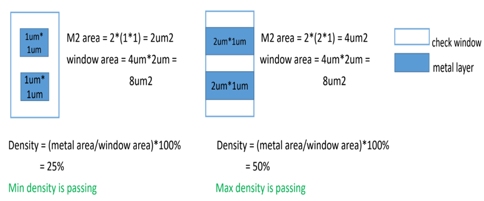
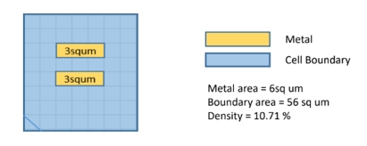
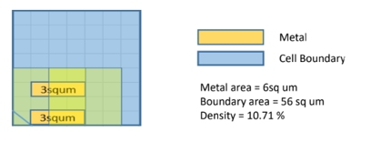
Density issues in VLSI layout design refer to the non-uniform distribution of features across the chip, which can significantly impact the manufacturing process and the performance of the final product. The layout pattern density over a region is defined as the ratio of the area occupied by rectangular shapes to the total area of that region, as shown in Figures 1.1 and 1.2.
Density = (Base/Metal/Via) area / Total area
Density constraints in VLSI layout design are typically represented in two distinct ways. They can be applied to the entire design area or specifically to the region covered by the checking window, which is moved incrementally across the design to detect localized density issues.
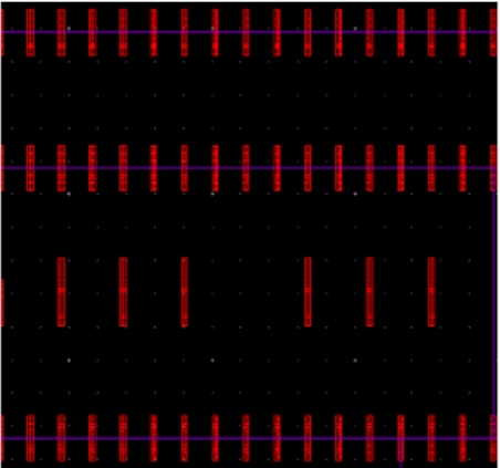
Figure 1.1: Before shapes fill flagging density issue
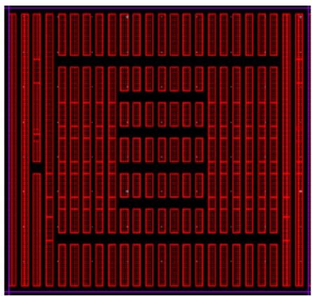
Figure 1.2: After shapes fill to fix density issue
Types of Density:
- Base density
- Metal density
- Via density
- Cumulative density
1. Base density: The ratio of the area occupied by base layers, such as poly and diffusion, to the total area of the base layers is expressed as a percentage. This percentage indicates how densely these poly and diffusion layers are packed on the chip. The uniformity of diffusion is strongly associated with processes like shallow trench isolation (STI) and rapid thermal annealing (RTA), which are integral to transistor formation. In 3D FinFET technology, the poly dummy fill is crucial because the height of the FinFET directly depends on the poly dummy density.
2. Metal density: The metal dummy is strongly associated with the Chemical Mechanical Polishing (CMP) process and significantly affects the interconnected RC parasitic. Inconsistent metal density across the chip results in varying amounts of dielectric layers between metal layers, leading to performance variations. To achieve uniform metal thickness and a flat surface after CMP, metal fills are necessary for maintaining consistent metal density. Uniform metal density helps to prevent common issues such as dishing and erosion. Metals, due to their mechanical softness compared to dielectrics, have surfaces that are prone to 'dishing', and very wide metal areas can experience thinning (erosion) shown in below figure 2.1. Additionally, dummy metal fill patterns can function as decoupling capacitors, shields, and aids in thermal distribution. Ensuring good metal density on the chip improves its planarity, benefiting subsequent metal layer deposition processes.
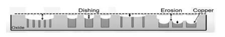
Figure 2.1
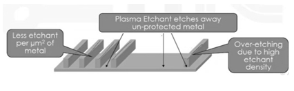
Figure 2.2
A narrow metal wire, when isolated from other metals, is exposed to a higher concentration of etchant compared to closely spaced wires, leading to potential over-etching of the narrow metal shown in figure 2.2. By using the minimum metal density rules, we can overcome this.
3. Via density: To meet the growing demand for better IC performance, new low-k dielectrics are being introduced to minimize RC delays in the BEOL (back end of line) interconnects. While these low-k dielectrics enhance electrical performance, they also reduce mechanical strength. This reduction in mechanical strength is particularly critical during packaging, where the BEOL undergoes high thermo-mechanical stresses due to differing coefficients of thermal expansion (CTE) between the silicon die and the packaging substrate during various processing steps, increasing the risk of the BEOL failure. To preserve the mechanical integrity of the BEOL, it is crucial to offset the reduced strength and stiffness of the low-k dielectrics employed.
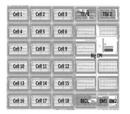
Figure 3.1: shows Test chip with 18 small cells, one big CPI test cell, two Through silicon via (TSV), & BEOL EM1 EM2 monitoring cells.
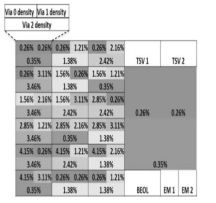
Figure 3.2: shows Via density (Via0, Via1, Via2) distribution along the test chip.
Effect of Via Density on the Mechanical Stability of Advanced BEOL Interconnects under Chip Package Interaction (CPI) is shown in Figure 3.2.
4. Cumulative density: The planarization and interlevel dielectric (ILD) thickness of a polished surface at one layer have a cumulative effect on the planarization and ILD thickness of subsequent higher layers. To ensure the desired manufacturability output after the CMP process, a dummy metal is inserted. The dummy metal fill provides a smoother surface planarity and better yield output.
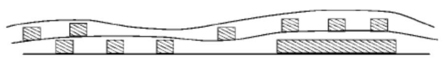
Figure 4.1: ILD planarization before dummy metal fill insertion
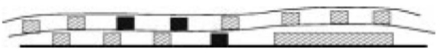
Figure 4.2: ILD planarization after dummy metal fill insertion (black tiles)
During fabrication, the variations in grain structure due to physical limitations are expected. In the nanometer regime, the lateral wire dimensions significantly impact the effective resistivity of interconnects. Research indicates that a wire over an area without underlying metal can exhibit higher resistance due to the upper metal layer conforming to the underlying layer's structure. Consequently, wire resistance becomes a function of the underlying density, showing a near-linear dependence of the metal2 layer on the metal1 layer. For a long wire across the chip, the underlying layer induces resistance variation, in addition to any dishing or erosion that may occur, further contributing to height variability.
Types of Density errors:
- Min density: Etching material tends to accumulate more in the gaps, leading to over-etching of the existing metal, which may create open circuits.
- Max density: Metal regions experience thermal expansion, which can cause insulators to crack and result in shorts or failures in chips.
The Min Density constraint, when paired with the Max Density constraint, helps ensure that the metal density in a design is maintained within an optimal range, avoiding both excessive sparsity and density. Conversely, the Max Density constraint, when used alongside the Min Density constraint, serves the same purpose, ensuring that the metal density does not become too dense or too sparse.
How is Density calculated?
The window is scanned across the whole chip with the given step size which is equal to half of the window size.
Example:
If the Min required M2 density in 2um*4um window is 20% and Max allowed M2 density in 2um*4um window is 80%.
Then,
To check density using a stepped value, begin at a corner of the design (as illustrated in figure 5.1) and assess the density percentage within an area (window) whose height and width are each twice the step size or equal to the window size. Move the window incrementally across the design by step size, verifying that the density percentage within each window remains within the maximum required value.
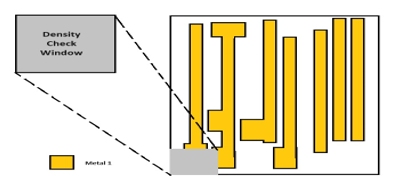
Figure 5.1
The maximum density difference between adjacent windows is expressed as a percentage between 0 and 100. For instance, if one window has a metal density of 80% and the maximum allowable density difference between adjacent windows is 10%, then the metal density in adjacent windows can vary between 70% and 90%. This ensures that the metal density difference between adjacent, non-overlapping density checking windows remains within the specified percentage range, as depicted in figure 5.2.
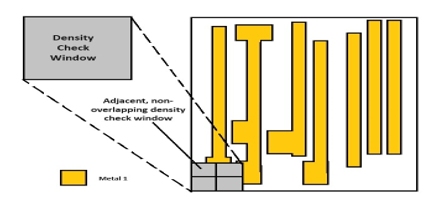
Figure 5.2
How does window scanning happen?
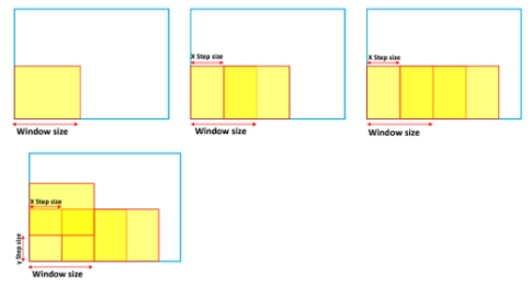
Figure 6
The window size is a predefined rectangular area used to scan the layout for density analysis. Step size determines the distance between the consecutive windows during the scanning process shown in Figure 6.
How Density certification can be validated?
Density certification is an important concept for a density black-boxed IP. When selecting a block for this purpose, a trade-off is made to ensure that the block is sufficiently large to qualify as a density black-box. The rule for determining eligibility for density certification is as follows: the size of the IP cells in either direction must be smaller than the minimum width of the top-level cell boundary as shown in Figure 7.
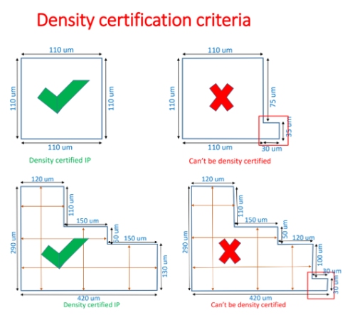
Figure 7
A black-boxed IP may be undersized by one density window. This undersized region is either black-boxed or excluded from density checks at the parent level. The part of the black-boxed IP that remains exposed for density checks at the next level is indicated by the red arrow. In some cases, density errors have been observed on a certified IP, and these errors are anticipated to occur within this one exposed window, as shown in figure 8.
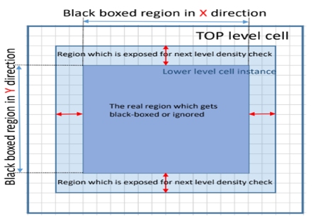
Figure 8
How to handle density error for certified and non-certified IP?
When the block is defined as certified IP, in this case this block itself must be cleaned with window/2 stepping, as shown below in Figure 9.1.
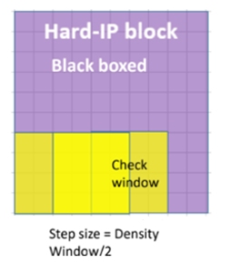
Figure 9.1
When the block is not defined as the certified IP, a strict density check will take place. Density will be cleaned using step size = 1 POD grid, as shown in Figure 9.2.
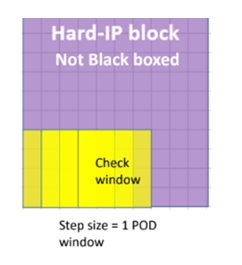
Figure 9.2
Why do we need to clean the density for each mask layer (Color Balancing) in FinFet?
- Layout decomposition, often referred to as layout coloring is a critical step in advanced semiconductor manufacturing, particularly in multi-patterning techniques like double-patterning lithography (DPL) or multi-patterning lithography (MPL), must generate divided patterns on separate masks while ensuring full compliance with process rules and avoiding any violations.
- Multipattern (MPT) coloring must not only produce split layouts without MPT conflicts but also ensure that pattern density is evenly distributed across the separate masks.
- Color balancing plays a crucial role in lithography and etching process control, helping to achieve consistent and uniform patterning quality.
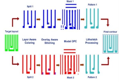
Figure 10: shows Double patterning using litho - etch- litho - etch process
Density Black Boxing:
- Memory consumption and runtime limitations can be mitigated by using a black-boxing mechanism.
- A trade-off is made when selecting a block that is large enough to be considered a density black box.
- Density certification is a crucial term used for IP that has been density black-boxed.
- IP refers to the user-defined cell(s) that are validated individually and then removed when placed hierarchically.
Types of Density flow checks:
1. Global density check: No specific window size or step size is provided; the density is calculated over the entire cell boundary. This means the density measurement encompasses the whole cell area rather than discrete windows or steps.
density = drawn data area/ area of top cell boundary
2. Local density check: When using a window size and step size, the step size is set to half of the window size. The density is calculated by comparing the data area within each window to the total window area. This method enables a comprehensive evaluation of density across the entire design.
density = drawn data area/ area of 1 check window
3. LDI: Local intermediate density check:
- Window size and step size are used.
- Window size is bigger than local density checks.
- Step size = window size/2
- Density gets calculated by taking the data area and window area.
density = drawn data area / area of 1 check window
- No guard band is applied for local intermediate density checks.
- Local intermediate density checks exist for base layer, via layer, metal layer.
- Local intermediate density checks have only min density checks.
4. CD: Concentrated density check:
- Window size and step size are used.
- Window size is smaller than local density checks.
- Step size = window /2.
- Target density is slightly bigger than local density checks.
- No guard band is applied for concentrated density check.
5. CM: Cumulative density check:
- Akin to CD checks + cumulative metal area gets accounted
- M5 density check = M5 + M6 + M7 + M8
- M6 density check = M6 + M7 + M8 + M9
- M7 density check = M7 + M8 + M9 + M10
- M8 density check = M8 + M9 + M10 + M11
- No guard band is applied for Cumulative density checks.
6. GRDEN: Global resistor template density check:
- Window size and step size are used.
- Step size = window/2 for all GRDEN checks.
- GRDEN certification requirement is different than LD, CD, CM density certification requirement.
- 100um*100um block size requirement is not valid for GRDEN certification.
- Oversized resistor array block should be fully inside the top cell boundary.
- Block itself must be standalone GRDEN clean.
Traditional density checks: Guard band approach
Guard band:
- It utilizes a step size that falls within the range of half the window size and the manufacturing grid
- A guard band of ±3% is applied to ensure the integrity and cleanliness of any skipped window
- Using the guard band approach, the minimum and maximum density rules are adjusted by ±3%, resulting in checks for 20.6% for minimum density and 77.6% for maximum density instead of the original 20% and 77%
- Guard band approach becomes more complex when applied to hierarchical designs
So, an additional guard band must be applied for hierarchical designs to account for their complexity.
Conclusion
Density issues are a critical concern in VLSI layout design, affecting the manufacturability, performance, and reliability of integrated circuits. By understanding the types and impacts of density variations, and employing effective density checking and mitigation techniques, designers can enhance the quality and yield of their designs. Advanced tools and methodologies, such as dummy fill insertion and optical proximity correction, play a vital role in addressing density challenges, ensuring that the final product meets stringent manufacturing standards.
References:
Rabaey, J. M., Chandrakasan, A., & Nikolic, B. (2003). *Digital Integrated Circuits: A Design Perspective* (2nd ed.). Pearson Education.
Yeh, C. T., Peng, H. L., & Lee, C. C. (2012). "Metal fill and its impact on advanced CMOS interconnect." *IEEE Transactions on Electron Devices*, 59(7), 1825-1832.
Cadence Design Systems. (2015). "Managing Metal Density Variations in Advanced Technology Nodes.
Synopsys, Inc. (2018). "Advanced Density Checking and Dummy Fill Solutions."
Authors:
Abhishek BV:

He has been working as a senior engineer at eInfochips for over two years, with a total of over 6 years of experience in analog layout design. He graduated in electronics & communication engineering. He has worked on various technology nodes, including 7nm, 10nm, 16nm, 40nm, 65nm, 130nm and 180nm in analog layout design.
Bhanu Rathore:

The author has over 10 years of experience in the microelectronics industry and is currently a lead engineer at eInfochips. Previously, the author held positions at NXP Semiconductor and Qualcomm. Specializing in analog mixed-signal layout design, the author has successfully led multiple high-level projects across various technologies. The author holds a postgraduate diploma in Embedded and VLSI Design from the Centre for Development of Advanced Computing (CDAC) Noida and a Bachelor of Technology in Electronics and Communication Engineering from Uttar Pradesh Technical University.