by Jin-Seok Hong, Goang-Seog Choi, Ki-Seon Cho, Ju-Seon Kim, Jum-Han Bae
Storage Solution Group, DM R/D Center, Samsung Electronics co. Ltd.
416, Maetan 3 dong, Paldal gu, Suwon, Korea
Abstract :
As designs are getting complicated, Industry needs IPs of multi-abstraction for partitioning flexibility, fast simulation speed, and various reasons. The truth, however, is that most HW IPs are written at RT-level and reused as it is. This problem made engineers to set up an intermediate flow to meet shortening time-to-market. So, we attempted to accumulate knowledge on legacy RT-level IP reuse by using recently emerging commercial co-design tool (CoWare N2C) and propose a possible approach, making advantage of interface-based design[1], platform-based design[2] concepts ,and etc while following a traditional flow at the same time.
From this case study, we assume that small scale of projects can still follow the traditional flow but tight schedule would make more verification missed on and on. In an intermediate phase prior to a true high level design, an introduction of commercial tools with features of platform generation and interface synthesis is considered to be reasonable to utilize abundant RT-level IPs.
1. Introduction
In an advent of SoC era, the industry has seeked new methodologies, languages and tools to handle the growing complexity of ICs and increasing SW portion in design. First in the field of system description language based on ANSI-C, many companies and non-commercial initiatives are driving standards and environments : Open SystemC Initiative[3], SpeC Technology Open Consortium[4], A|RT designer / builder from Adelante, Cyn++ from Forte, OCAPI from IMEC, BACH from Sharp ,and etc. Â
In addition to this C-based system description trend, commercial tools associated with their unique methodologies for the high-level design were introduced : VCC from Cadence, N2C[5] from CoWare, Foresight from Foresight, eArchitect from Innoveda, Virtio from Virtio ,and etc.
New system description languages, commercial tools for high-level design and methodologies are considered to be necessary in SoC making companies, but there is not much knowledge on abundant legacy IPs reuse in these environments.
In this paper, we first present a brief description of ATA/ATAPI, CoWare N2C ,and AXIS RCC before two distinct approaches to reuse legacy RT-level IPs are elaborated. The one of the two approaches is for conventional flow and the other for co-design tool-based flow using CoWare N2C. After these two approaches, we propose a practical flow based on related issues and measured numbers from our experiments. Finally, lessons from a legacy RT-level ATAPI IP reuse are given.
2. ATA/ATAPI
ATA/ATAPI are the real names for the mass storage device interface that is frequently called IDE and EIDE[6]. ATA has been employed mainly for HDD and extended to cover optical devices such as CD and DVD. The extended version of ATA is ATAPI (AT Attachment with Packet Interface).
Since ATAPI interfaces with host machines like PC, a host model as well as an embedded FW (Firmware) is needed to design and verify an ATAPI IP. The host model issues ATAPI commands and makes ATAPI do appropriate actions. Some commands are entailed with massive and burst data transfer while some require the exchange of simple information between a host and an ATAPI.
3. CoWare N2C & AXIS RCC
CoWare N2C is a tool and methodology that enables system description, partitioning, interface synthesis, simulation ,and link-to-implementation. ANSI C-based CoWare C is used to describe system while externally developed codes using C, VHDL ,and Verilog languages can be imported for co-simulation. It has strength in both platform-based design and interface-based design.
With a patented RCC technology, AXIS provides HW accelerator products of reasonable performance. Commercial FPGAs are integrated in a chassis and need long compilation time to make acceleration ready compared to processor based accelerator or HW simulator on workstations.
4. Conventional IP Reuse Flow (Real Case)
The chip implemented in a conventional flow, Figure 1, consists of analog, digital ,and memory cores as well as a small DSP processor and amounts to about 2 million gates in size. We followed commonly used ASIC design flow, fabricated it in 0.18 process technology and is testing the chip.
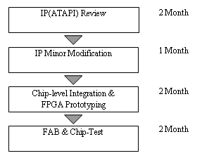
Figure 1: Conventional flow
Most IP blocks except for ATAPI have been previously used and maintained inside our division from invention. The newly integrated ATAPI IP was written in RT-level Verilog („l 80000 gates) and delivered only with a brief register description from the outside. The following figure show how the new chip is configured (Figure 2).
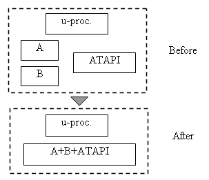
Figure 2. Chip Configuration
This kind of simple IP integration, excluding the external micro-processor, took three extra months for IP review and minor modification, as shown in Figure 1, due to the slow performance of HDL simulation engines (~ 100 Cycle/Sec). Because of the late integration, a lack of models including the micro-processor, slow simulation speed, and deficient debugging features, SW engineers could not begin their development effort until a new system was prototyped with FPGAs.
In this project, using a conventional flow approach did not provide enough time to verify the integrity and simulate every possible scenarios due to tight schedule and slow simulation environment. Unfortunately, SW engineers could not suggest any improvements in the system and did not even know if SW would run on the chip without any problems due to functionality or performance.
5. New IP Reuse Flow using a co-design tool ( focusing on legacy RT-level IP  reuse )
In this section, we present an approach using a co-design tool for a case that more than one processor are embedded and abstraction level of some IPs are fixed at RT Level. For this purpose, we chose N2C from CoWare as a co-design tool and used NC-Verilog from Cadence (event driven simulator) , XSIM from AXIS (cycle based simulator), RCC (HW accelerator) from AXIS as HW simulation tools.
The figure 3 shows how the ATAPI IP is used in our case.
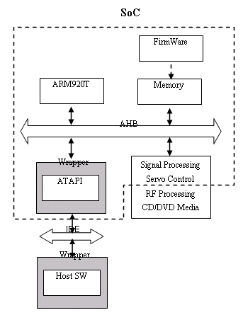
Figure 3. Co-design Tool-Based Approach
The above ARM920T & AHB-Bus Platform (commonly called ¡¥base architecture¡¦) written in multi-abstraction levels is qualified and provided from CoWare. As seen above in Figure 3, two SW IPs such as Host SW and Embedded FW are written in C, but Host SW has no base architecture on which it runs while FW is compiled for ARM920T ISS model and loaded on an embedded memory. The rest IPs and analog/mechanic models are simplified to focus on ATAPI integration and will possibly be replaced with more detailed ones. Around 1 man-month was used to set up this whole virtual system.
Several notable issues were listed while creating this system.
1) Interface mismatch between IPs (ex. ad-hoc IP specific protocol vs. AHB bus protocol)
Most of legacy IPs have their own protocols. So, they are possibly connected only to IPs with the same protocol. To tackle this interface mismatch in simple ways, wrapper can be added on top of the existing protocol of legacy IPs sacrificing some performance. The other better but costly approach is to replace the IP specific protocol with the counter-part protocol. This replacement scheme looks simple but is very painful in a case that interface and internal behavior are entangled. As two methods may be solutions in a pending project or a specific case, repeated modifications are inevitable case by case and project by project.
For this issue, we chose to apply interface synthesis provided by CoWare N2C, Figure 4. The tool helps to connects IPs automatically if the interface of IP complies with tool-defined protocols, or ¡¥primitive protocols¡¦. As matching IP interfaces needs manual effort, modification of ad-hoc protocols into primitive protocols should be done at least one time. The main benefit from using interface synthesis is that we do not need to rework interface case by case, which finally leads to shorter time-to-market in derivative products. However, a kind of translation block in between IPs, called ¡¥bridge¡¦ is placed as a consequence of interface synthesis, which brings up some performance loss.
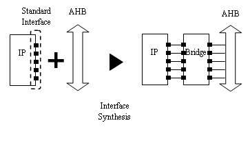
Figure 4. Interface Synthesis
2) Slow simulation speed due to RT-level IPs
The set-up environment involves not only glue logics but also a processor. When all models are simulated together, a bottleneck in simulation speed goes to the HW simulation side for the glue logics. Therefore, early involvement of SW engineers for co-development becomes meaning-less.
Our experiment showed that mixed C and HDL co-simulation provides a clean path for migrating existing IP in HDL format, but does not provide a fast enough simulation environment. In order to improve performance more of the HDL blocks need to be converted to higher abstracted models. Due to the lack of performance in a co-simulation environment, the software developers still use FPGA approach.
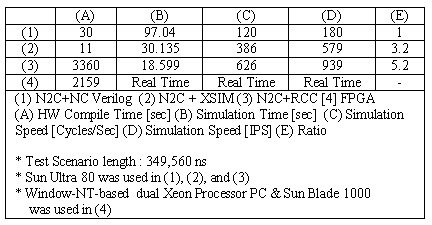
Table 1. Simulation VariantsIn the table 1, we note that any environment is not fast enough to make HW-SW co-development feasible. Anyhow, HW simulation should be improved continuously to render these environments more suitable to design than verification. As shown by another project, if you move all HDL blocks to a register transfer C abstraction level, the simulation performance improves to two thousand instructions per second.
3) Verification scheme for RT-level IPs¡¦ integration with the given platform like ARM7TDMI + AMBA
This last issue is related to complexity. Since integrating and verifying all RT-level & qualified IPs at once slows down simulation sharply and increases complexity as well, IPs except for a design under integration and verification can be swapped with appropriate models, as shown in Figure 5. Once the design under test is proven, each IP will in turn, be replaced by the RT-Level equivalent model, while the rest of the design is at an abstracted or simplified model. We call it a successive verification.
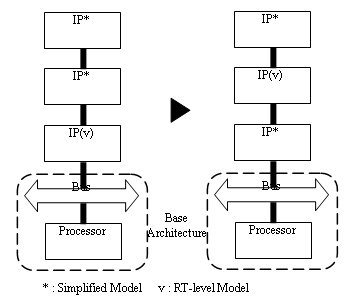
Figure 5. Successive Verification
6. A proposed flow
Considering all the above issues, we suggest a flow in figure 6 to maximize the efficiency of legacy RT-level IP reuse.
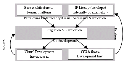
Figure 6. Intermediate Design Flow
A base architecture is a kind of skinny platform which comprises a combination of processors, buses, OS, and SW development tools. These elements in the base architecture are configurable and extendable by co-design tools. Meanwhile, the former platform means the system that was developed in the previous generation. So, various HW or SW IPs can be already added to a base architecture in a former platform. The important thing is that they are flexible and already proved as well.
IPs inherently exist in a variety of styles. For example, HW IP, SW IP, RT-level verilog IP, RT-level C IP ,and etc. For legacy RT-level IPs that we have interest in, the interface of IP is assumed to be maintained according to interface-base design concept, or specifically protocols that are ready for interface synthesis.
After base architectures / former platforms and required IPs are ready, an integration and verification stage follows. Interface synthesis is utilized to integrate IPs and most of verification focuses on integrity itself, when the successive verification scheme is used to reduce complexity. From our experiments, we found out that virtual development environments can be acceptable at this stage if a successive verification scheme and appropriate HW simulation boost are prepared.
Although virtual development environments provided by co-design and co-verification tools are useful in some cases, the performance for SW development environments is by far low. Since accuracy and simulation speed of IP models for virtual development environments have a limit, FPGA-based development environments are considered while virtual development environments are utilized at specific concerns.
One of the crucial points in the flow is that the whole process can be quickly iterative. As designs are getting bigger and complicated, there will more demands to respin to the previous design stage frequently for various reasons. So, we measured time for virtual system creation in CoWare N2C in 3 cases. Even though the table 2 does not include the time to implement the generated virtual system in FPGA, the result seems notable.
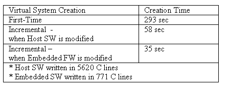
Table 2. Virtual System Creation
7. Lessons
Through the co-design tool based approach, we can present our lessons as follows.
1) Early proven and formal platforms of multi- abstractions are necessary to focus on IP integration and system-level development
When we design a new application, an emphasis should be put on newly implemented IPs. Therefore, the platform, on which new IPs are integrated, is recommended to be early proven, formal, and of multi-abstractions.2) Co-design tools with interface synthesis and 3rd party simulator link features help easy IP integration and fast system extension.
Tools to support interface synthesis and 3rd party simulator link features are crucial as noted earlier. Maintaining interface to be handled by tools embodies interface-based design. In addition to interface concern, IPs even with the well-defined interface can be written in different languages. If these IPs can not be imported and simulated directly inside co-design tools, 3rd party simulators should be able to be linked to the tools.3) IP modification to be conformable to standard interface ( recognized by tools ) is needed in order to give IP flexibility
The flexibility of IP here is related to how easily IPs are connected to one another. Formal or standard interfaces can let tools automatically integrate IPs. We believe that the concept interface-based besign and the standard SLIF[7] from VSIA are helpful generally. In the tool CoWare N2C that we used, the standard interface is called ¡¥Primitive Protocols¡¦4) Cycle Based Simulators, HW Accelerators, HDL-to-C Conversion are needed for HW simulation speed boost.
For multi million gate SoCs, we believe that it is the best way to make every IP from top to bottom in a consistent way. But the current situation does not allow it. So, Cycle based simulators, HW accelerator, and HDL-to-C conversion may be good alternatives for simulation speed boost with a minimum of IPs at RT-level when we do simulations.5) SW development on the early integrated virtual system has great impact on system quality and time-to-market.
As SoC is getting evolved, SW portion in design is growing fast. It means that co-development of HW and SW affects SoC severely in various perspectives. But it is currently very hard to provide virtual development environments which are fast and accurate enough to meet SW engineers¡¦ flavor.
So, we had better categorize verification points. A certain category of verification is best simulated and proved in virtual development environments while SW engineers prefer to use fast FPGA environments.
8. Conclusions
Nowadays, methodologies and tools to implement SoCs from high-level languages are beginning to emerge and engineers are asked to make IPs with multi abstractions. However, industry seems not to be ready to make a paradigm shift over-night. So, we believe that a flow with a combination of formal platforms, abundant legacy IPs and commercial tools will be reasonable for a while. This intermediate flow is assumed to play a role of bridge to high-level design paradigm using more flexible IPs.
9. References
[1] J. Rawson, A. Sangiovanni Vincentelli, Interface Based Design, Proc. of Design Automation Conf., June 1997
[2] Henry Chang, Grant Martin, et al., Surviving the SoC Revolution : A Guide to Platform-Based Design. Kluwer Academic Publishers, USA, 1999.
[3] Synopsys Inc., CoWare Inc., Frontier Design, Inc. SystemC User¡¦s Guide, 2000.
[4] D. Gajski, J. Zhu, R. Doemer, A. Gerstlauer, and S. Zhao. SpecC : Specification and Methodology. Kluwer Academic Publishers, Boston / Dordrecht / London, 2000.
[5] www.coware.com
[6] www.ata-atapi.com
[7] VISA, VSI Alliance System-Level Interface Behavioral Documentation Standard v 1.0, www.vsi.org, March 2000
