by You-Pang Wei and Bill Wasserman, Legend Design Technology, Inc.
Santa Clara, California, U.S.A.
Abstract :
SoC designs are becoming more memory dominant. Due to sophisticated design, sensitivity to technology and complicated integration, memory IP needs to be characterized and validated by taking into account reliability issues such as glitches, metastability, timing soft error, noise margin, etc. Reliability-based characterization of memory IP can ensure maximum yield and manufacturability of high performance low power SoC designs.
Introduction
It is forecasted that by the year 2014, embedded memory will occupy 94% of the total area on the chip [1], allocating a mere 6% for reused logic or new logic designs. In System-On-a-Chip (SOC) designs, a variety of memories, logic and control functions are being integrated onto a single chip. Designers have access to a large variety of memory types and sizes. It is now common to see over 200 different configuration blocks of SRAM, Register Files, ROM and other specialty memories placed on a single SOC design.
Today’s technology is also moving rapidly from 0.25µm, 0.18µm, 0.15µm 0.13um to the current 90nm (and below!). Generic CMOS, not being lagged behind, has also diversified into several variants such as high speed, low power and high density. Most importantly, each and every process variant now has its own characterization. With high volume production it is common to manufacture a part at several foundries to meet the customer needs. Since each process variant at each foundry is slightly different, it is necessary to re-characterize memory for the specific process and foundry to be used – this to ensure desired performance and silicon yield.
Design houses are starting to approach multiple vendors and multiple sources for their embedded memory requirements. This has brought with it a new class of integrity issues. To fully utilize the embedded memories in their IC designs, accurate timing and power models are essential [2][3]. Quality validation and re-characterization is necessary for the memories used at different PVT (process, voltage and temperature), especially for high-speed and low power designs.
Complete Solution: CharFlo-Memory!TM
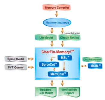
There are three phases in a memory development flow: Design, Verification, and Characterization. Memory characterization is the process of building up a timing and power model of the memories. The market now demands high performance and a short product time-to-market. Legend's CharFlo-Memory!TM products, which include MSLTM, SpiceCutTM, and MemCharTM, automate the time consuming and error prone processes associated with characterization and verification of embedded memory (custom and commercially available IP, i.e. Artisan, Virage, TSMC, Faraday, Dolphin Technology, VeriSilicon … [5][6][7]) . The flow of CharFlo-Memory!TM is shown in Fig. 1.
MSLTM is designed to facilitate an efficient layout-based .LIB in, .LIB out characterization and verification flow [4] for compiler generated memories. For each instance, a memory compiler produces a ‘.Lib’ file with information such as pin names, slopes and loading for timing models etc. MSLTM reads in the ‘.Lib’ file, and automatically generates the controls for running SpiceCutTM and MemCharTM. In addition, MSLTM will update the ‘.Lib’ file model after characterization and simulation are completed.
SpiceCutTM [8] is the optimized tool for memory circuit reduction and is the most important part of the CharFlo-Memory!TM solution. MemCharTM configures and manages the characterization work. As technology advances, circuits become more complex. The process of characterization often exposes the limitations of extraction tools and simulators – especially for large memories. Designers are looking for an efficient solution for performing the extraction work. However, simulators take a long time to simulate the large extracted memories. To improve the extraction time for large memory instances engineers can use the memory compiler or layout editor to cut the memory array into a ring-shape. SpiceCutTM has the intelligence to emulate the extracted ring-shape memory array to full size when it builds critical path circuits – with no loss of accuracy [10]. The optimized critical path circuits represent a 98% reduction in the netlist size that needs to be simulated for the timing and power parameters.
MemCharTM [9] accepts the specification for each parameter from the memory datasheet and the extracted SPICE netlist of the memory circuit as its inputs. It automatically generates the stimulus and controls based upon the specifications, and then its internal Circuit Simulation Manager will be called upon to administer simulations automatically in ‘sweep’ loops or in ‘optimization’ loops. A final timing table will be generated and used for VerilogTM or PrimeTimeTM simulation.
Consider the future technology prediction that 94% of an SOC design area will be occupied by embedded memory [1]. If designers could remove the uncertainty associated with embedded memories, they would have gained a considerable competitive edge. This illustrates the importance of having an accurate and efficient methodology in place for memory characterization.

Fig. 1 Diagram illustrating Legend’s methodology of memory characterization
Instance model versus Compiler Model
Memory compilers can generate several hundred thousand different size instances. Since it is next to impossible to characterize each and every one, what is commonly done is that compiler providers characterize only the largest, the smallest, and selected cases in-between. The resulting compiler model is based upon interpolation and extrapolation from those original ‘grid’ characterizations, which often introduces significant error to the actual results [11].
As shown in Fig. 2, the interpolation error of the compiler’s table-lookup model might represent the timing values as being less than actual silicon. This uncertainty can lead to failure or low yield.
As shown in Fig. 3, the margin could then be added to the model for protection. However, the added margins might make the timing from compiler’s table-lookup model slower than actual silicon. The performance is then sacrificed.
This is the reason why instance characterization is preferred. Instance characterization provides an accurate timing model for every memory instance generated [2][3]. The compiler’s timing model can be fine-tuned for optimal performance and also it serves as a ‘what- if’ analysis for failure prevention.

Fig. 2 Compiler table-lookup model without margin.

Fig. 3 Compiler table-lookup model with margin added
Push-Button Characterization for Commercial Memory Compiler Users
Commercial memory compiler users utilize the compiler table-lookup models provided by vendors. Compiler generated table-lookup models are normally based upon specific process corners, power supply and temperature. This is unlike a CharFlo-Memory!TM produced optimized instance model that reflects the silicon reality and can be characterized for any configuration at any process corner. The reasons for instance based models are:
Updating the timing and power models for any PVT (process, voltage and temperature)
Santa Clara, California, U.S.A.
Abstract :
SoC designs are becoming more memory dominant. Due to sophisticated design, sensitivity to technology and complicated integration, memory IP needs to be characterized and validated by taking into account reliability issues such as glitches, metastability, timing soft error, noise margin, etc. Reliability-based characterization of memory IP can ensure maximum yield and manufacturability of high performance low power SoC designs.
Introduction
It is forecasted that by the year 2014, embedded memory will occupy 94% of the total area on the chip [1], allocating a mere 6% for reused logic or new logic designs. In System-On-a-Chip (SOC) designs, a variety of memories, logic and control functions are being integrated onto a single chip. Designers have access to a large variety of memory types and sizes. It is now common to see over 200 different configuration blocks of SRAM, Register Files, ROM and other specialty memories placed on a single SOC design.
Today’s technology is also moving rapidly from 0.25µm, 0.18µm, 0.15µm 0.13um to the current 90nm (and below!). Generic CMOS, not being lagged behind, has also diversified into several variants such as high speed, low power and high density. Most importantly, each and every process variant now has its own characterization. With high volume production it is common to manufacture a part at several foundries to meet the customer needs. Since each process variant at each foundry is slightly different, it is necessary to re-characterize memory for the specific process and foundry to be used – this to ensure desired performance and silicon yield.
Design houses are starting to approach multiple vendors and multiple sources for their embedded memory requirements. This has brought with it a new class of integrity issues. To fully utilize the embedded memories in their IC designs, accurate timing and power models are essential [2][3]. Quality validation and re-characterization is necessary for the memories used at different PVT (process, voltage and temperature), especially for high-speed and low power designs.
Complete Solution: CharFlo-Memory!TM
There are three phases in a memory development flow: Design, Verification, and Characterization. Memory characterization is the process of building up a timing and power model of the memories. The market now demands high performance and a short product time-to-market. Legend's CharFlo-Memory!TM products, which include MSLTM, SpiceCutTM, and MemCharTM, automate the time consuming and error prone processes associated with characterization and verification of embedded memory (custom and commercially available IP, i.e. Artisan, Virage, TSMC, Faraday, Dolphin Technology, VeriSilicon … [5][6][7]) . The flow of CharFlo-Memory!TM is shown in Fig. 1.
MSLTM is designed to facilitate an efficient layout-based .LIB in, .LIB out characterization and verification flow [4] for compiler generated memories. For each instance, a memory compiler produces a ‘.Lib’ file with information such as pin names, slopes and loading for timing models etc. MSLTM reads in the ‘.Lib’ file, and automatically generates the controls for running SpiceCutTM and MemCharTM. In addition, MSLTM will update the ‘.Lib’ file model after characterization and simulation are completed.
SpiceCutTM [8] is the optimized tool for memory circuit reduction and is the most important part of the CharFlo-Memory!TM solution. MemCharTM configures and manages the characterization work. As technology advances, circuits become more complex. The process of characterization often exposes the limitations of extraction tools and simulators – especially for large memories. Designers are looking for an efficient solution for performing the extraction work. However, simulators take a long time to simulate the large extracted memories. To improve the extraction time for large memory instances engineers can use the memory compiler or layout editor to cut the memory array into a ring-shape. SpiceCutTM has the intelligence to emulate the extracted ring-shape memory array to full size when it builds critical path circuits – with no loss of accuracy [10]. The optimized critical path circuits represent a 98% reduction in the netlist size that needs to be simulated for the timing and power parameters.
MemCharTM [9] accepts the specification for each parameter from the memory datasheet and the extracted SPICE netlist of the memory circuit as its inputs. It automatically generates the stimulus and controls based upon the specifications, and then its internal Circuit Simulation Manager will be called upon to administer simulations automatically in ‘sweep’ loops or in ‘optimization’ loops. A final timing table will be generated and used for VerilogTM or PrimeTimeTM simulation.
Consider the future technology prediction that 94% of an SOC design area will be occupied by embedded memory [1]. If designers could remove the uncertainty associated with embedded memories, they would have gained a considerable competitive edge. This illustrates the importance of having an accurate and efficient methodology in place for memory characterization.

Fig. 1 Diagram illustrating Legend’s methodology of memory characterization
Instance model versus Compiler Model
Memory compilers can generate several hundred thousand different size instances. Since it is next to impossible to characterize each and every one, what is commonly done is that compiler providers characterize only the largest, the smallest, and selected cases in-between. The resulting compiler model is based upon interpolation and extrapolation from those original ‘grid’ characterizations, which often introduces significant error to the actual results [11].
As shown in Fig. 2, the interpolation error of the compiler’s table-lookup model might represent the timing values as being less than actual silicon. This uncertainty can lead to failure or low yield.
As shown in Fig. 3, the margin could then be added to the model for protection. However, the added margins might make the timing from compiler’s table-lookup model slower than actual silicon. The performance is then sacrificed.
This is the reason why instance characterization is preferred. Instance characterization provides an accurate timing model for every memory instance generated [2][3]. The compiler’s timing model can be fine-tuned for optimal performance and also it serves as a ‘what- if’ analysis for failure prevention.

Fig. 2 Compiler table-lookup model without margin.

Fig. 3 Compiler table-lookup model with margin added
Push-Button Characterization for Commercial Memory Compiler Users
Commercial memory compiler users utilize the compiler table-lookup models provided by vendors. Compiler generated table-lookup models are normally based upon specific process corners, power supply and temperature. This is unlike a CharFlo-Memory!TM produced optimized instance model that reflects the silicon reality and can be characterized for any configuration at any process corner. The reasons for instance based models are:
- Providing accurate timing and power models for high speed and low power designs.
Push-Button Characterization for In-house Memory Compiler Development
The conventional approach to characterizing embedded memories requires engineers to manually locate the critical paths and generate the simulation stimulus for the characterization work. Many simulations are run and then extensive analysis is done to draw conclusions for the timing models. The limitations of this methodology are apparent in deep submicron designs - 0.18 and below. The bigger timing tables need be run to verify design specifications. The manual work is time-consuming, error-prone and the results obtained are too conservative. To stay competitive, more and more memory compiler development teams have come to the realization that they need a tool that can provide an efficient and accurate memory characterization flow.
The tool has to handle unique characterization requirements and manage simulations for the memories generated from the memory compilers. It also has to be compatible with different circuit simulators including in-house spice simulators. It must provide a white box analysis environment, accurate timing analysis, and the automation capacity to complete the characterization flow.
CharFlo-Memory!TM is an ideal solution for a memory compiler development team [5][6][7]. Once the MSL configuration file is created for the compiler, it facilitates efficient instance based characterization. In measuring the throughput of the entire characterization process, the total CPU time used is important. Since characterization involves hundreds of simulations, the bottleneck in simulation time is due to the size of the memory circuit. The SpiceCutTM circuit reduction tool, which is a module in CharFlo-Memory!TM, builds optimized critical path circuits and also accounts for critical coupling effects. Its built-in AWE RC-reduction capacity can be used for additional effectiveness. In addition, CharFlo-Memory!TM can work with various commercial and in-house simulators. All this contributes to a high efficiency in-house characterization flow.
Reliability Checking in Characterization
With increasing design complexity and rising clock frequencies, reliability issues such as glitches and noise margin pose a big problem for memory designers and users.
To solve the problem manually is a daunting and undesirable task. It requires a great deal of engineering time and the results are doubtful. CharFlo-Memory!TM provides a transparent analysis environment, which allows users to debug and optimize the designs. CharFlo-Memory!TM not only recognizes the latches inside the embedded memories for glitch and noise analysis, but also performs the characterization based upon multi-criterion:
1. Glitches and MetaStability Prevention
As IC designs are getting more complicated, the ‘glitch’ and ‘metastability’ problem become critical - impacting both reliability and performance. This is especially true for memory designs. Since the glitches and metastability are embedded internally they can not be observed at the pins; it is extremely difficult to debug the error. CharFlo-Memory!TM can help to prevent the problems during characterization.
The example in Fig. 4 shows that if the hold time is too short (100 ps), it will induce glitches in internal nodes of latches (Q and QB). With the true hold time (300 ps), it can prevent glitches from happening.
To achieve optimal performance of a memory, there must not be any glitches or metastability. In the past, characterization was done uni-criterion. But with CharFlo-Memory!TM, it not only checks for correct functions but also performs glitch and metastability prevention.

Fig. 4 Characterization with ‘glitch’ prevention
2. Timing Soft Error Prevention
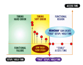
Timing soft error is defined as the event where access time increases due to a smaller or tighter constraint on the setup time of the input pins, as shown in Fig. 5. ‘Timing soft error’ has adversely impacted the reliability and performance of modern circuit designs. The ‘timing hard error’ causes hard failure and can be easily observed at the pins. However, timing soft error is caused by internal behavior such as racing in multiple paths and glitches in latches. It is extremely difficult to locate and debug the error; especially since the glitches disappear after propagating through two or three logic levels. For an experienced memory designer, it could take days and numerous simulations to discover the problem. And, to solve it could take another few weeks. As a result, the chip design may not meet performance targets and the silicon yield may be low.
CharFlo-Memory!TM, provides a ‘push-button’ solution for engineers to locate the ‘true’ setup and hold time and prevent the timing soft error problem.

Fig 5 Numerous simulations were performed to illustrate the impact of ‘Timing Soft Error’.
3. Noise Margin Consideration
Sense amplifier input is the voltage difference of Bit and BitB and is sensed by a pulse signal, as shown in Fig. 6. Internal noise could override the sensed signals if they are too small and cause the false data outputs. In Fig. 7, it has indicated
CharFlo-Memory!TM provides design margin check of ‘sense-amplifier input’ versus ‘noise margin’ across exhaustive patterns as shown in Fig. 8.

Fig. 6 Sense amplifier input is the voltage difference of Bit and BitB and controlled by sensing control signal

Fig. 7 Early sensing may cause reliability issues

Fig. 8 Exhaustive noise margin verification
Conclusion
Technology is moving rapidly and has diversified into variants such as high speed, low power and high density. Each process variant must have its own characterization. This has created the need for an automatic memory IP characterization tool.
Furthermore, to ensure the yields and manufacturability, the memory IP characterization tools need to take into account reliability issues such as glitch, metastability, timing soft error and noise margin etc. The CharFlo-Memory!TM toolset is the industry’s first reliability-based memory IP characterization software product and - most importantly - is silicon proven [7].
References:
As IC designs are getting more complicated, the ‘glitch’ and ‘metastability’ problem become critical - impacting both reliability and performance. This is especially true for memory designs. Since the glitches and metastability are embedded internally they can not be observed at the pins; it is extremely difficult to debug the error. CharFlo-Memory!TM can help to prevent the problems during characterization.
The example in Fig. 4 shows that if the hold time is too short (100 ps), it will induce glitches in internal nodes of latches (Q and QB). With the true hold time (300 ps), it can prevent glitches from happening.
To achieve optimal performance of a memory, there must not be any glitches or metastability. In the past, characterization was done uni-criterion. But with CharFlo-Memory!TM, it not only checks for correct functions but also performs glitch and metastability prevention.

Fig. 4 Characterization with ‘glitch’ prevention
2. Timing Soft Error Prevention
Timing soft error is defined as the event where access time increases due to a smaller or tighter constraint on the setup time of the input pins, as shown in Fig. 5. ‘Timing soft error’ has adversely impacted the reliability and performance of modern circuit designs. The ‘timing hard error’ causes hard failure and can be easily observed at the pins. However, timing soft error is caused by internal behavior such as racing in multiple paths and glitches in latches. It is extremely difficult to locate and debug the error; especially since the glitches disappear after propagating through two or three logic levels. For an experienced memory designer, it could take days and numerous simulations to discover the problem. And, to solve it could take another few weeks. As a result, the chip design may not meet performance targets and the silicon yield may be low.
CharFlo-Memory!TM, provides a ‘push-button’ solution for engineers to locate the ‘true’ setup and hold time and prevent the timing soft error problem.

Fig 5 Numerous simulations were performed to illustrate the impact of ‘Timing Soft Error’.
3. Noise Margin Consideration
Sense amplifier input is the voltage difference of Bit and BitB and is sensed by a pulse signal, as shown in Fig. 6. Internal noise could override the sensed signals if they are too small and cause the false data outputs. In Fig. 7, it has indicated
- Early sensing causes small V(Bit-BitB) and fast access time, but potential reliability issues.
- Late sensing causes large V(Bit-BitB) and slow access time, but with safer margins.
CharFlo-Memory!TM provides design margin check of ‘sense-amplifier input’ versus ‘noise margin’ across exhaustive patterns as shown in Fig. 8.

Fig. 6 Sense amplifier input is the voltage difference of Bit and BitB and controlled by sensing control signal

Fig. 7 Early sensing may cause reliability issues

Fig. 8 Exhaustive noise margin verification
Conclusion
Technology is moving rapidly and has diversified into variants such as high speed, low power and high density. Each process variant must have its own characterization. This has created the need for an automatic memory IP characterization tool.
Furthermore, to ensure the yields and manufacturability, the memory IP characterization tools need to take into account reliability issues such as glitch, metastability, timing soft error and noise margin etc. The CharFlo-Memory!TM toolset is the industry’s first reliability-based memory IP characterization software product and - most importantly - is silicon proven [7].
References:
