Overview
Few challenges facing the electronics industry today are more important than power management. Several factors are combining to place demands for lower-power operation on many types of consumer and business products. The traditional methods to control power have significant limitations; a new approach is sorely needed. This paper will:
- Provide background on the power management problem and some of the established solutions,
- Present the emerging technology of power islands as an alternative with several attractive features
- Describes Mobilizeâ„¢, the new power management
IP offering from Virtual Silicon that enables the incorporation of power islands into a wide variety of system-on-chip (SoC) designs.
The Power Crisis
Industry publications frequently refer to the “power crisis†in semiconductor design. When it comes to power management, the maxim for designers might well be “if it’s not a problem now, it soon will be.†The demand for low-power, or at least lower power, operation is arising in nearly every area of electronics. With so many factors at work, designers must be aware of end-product power requirements and should be looking proactively for effective solutions. The need for better power management is driven by three factors: mobility, process technology and SoC complexity.
The most obvious driver for low-power requirements is the tremendous increase in the demand for mobile electronics for both portable consumer electronics and business. Not only are more products going mobile, but they are becoming more complex with advanced color displays, wireless technology and increased storage. By their very nature, portable devices operate on battery power for the majority of their lives. Although advances in battery technology over the last ten years have been quite impressive, it appears that the demand for longer mobile life is currently outpacing the ability of battery manufacturers to innovate. Further, advancing battery technology is only one way to extend product operating life.
As one example, consider the laptop computer. Ten years ago, a battery life of one hour was considered state-of-the-art. Laptop users routinely carried an extra battery or two, adding considerable extra weight but extending the usability of the laptop only long enough for a medium-length commuter flight.
Five years ago, battery lifetimes had increased somewhat but most travelers needing longer periods between recharging opted for smaller, less versatile pocket computers or made do with the limitations of personal digital assistants (PDAs). Today, laptop battery lives of three to five hours are commonplace yet the demand continues to increase. The goal of having a full-featured laptop that can run for an entire day or a long coach flight (10-14 hours) remains elusive.
A similar history can be related for all manner of portable consumer devices. Cellular telephone users would like to recharge only once a week and parents would like their children to enjoy their game players for weeks without doling out new batteries. One of the hottest new technologies in years, MP3 players, can hold literally thousands of songs but most play no more than a hundred or so before running out of power.
Advances in process technology have also placed greater demands on power management. As finer geometry devices have been developed, the trend has been to reduce operating voltages. This trend has had the beneficial side effect of reducing power consumption. However, voltage levels seem to be stabilizing in the 1.0-1.2 V range for deep submicron technologies, which means that future technologies will not automatically result in power savings.
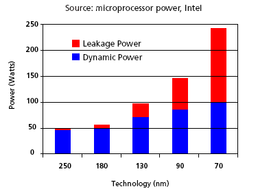
Power requirements are also affected dramatically by leakage currents. As shown in Figure 1, leakage consumes a greater and greater percentage of total power as feature size shrinks. By 130 nm, leakage is no longer a negligible factor and by 90 nm, leakage accounts for nearly half of total power consumption. Lowering voltage and turning off logic entirely are the most common ways to reduce leakage currents; this requires fine-grained power management inside the SoC.

Figure 1: Increasing Impact of Power Consumption
Of course, power demands are also growing with the sheer size and complexity of contemporary SoC devices. The enormous increase in functionality for each new generation of chip can more than offset the smaller size of the transistors, resulting in die size growth and nearly always a significant increase in power consumption.
Other less obvious factors influence electronics products as well. The so-called “green†initiatives, especially in Europe, have placed greater pressure on manufacturers of desktop computers and related products to reduce power consumption. Turning off an inactive screen is well-established technology but turning off a PC is rarely an acceptable solution. Even when the user is not actively typing on the keyboard or moving the mouse, it is common today for computers to run background applications such as:
- Continual checks for new email, instant messages or alerts (stocks, weather, etc.)
- Scheduled checks for O/S updates, virus definition updates, disk cleanup, backups, etc.
- Streaming audio or video that the user wants to continue even if not at the computer
The ability to reduce power while keeping essential services active suggests that a more fine-grained form of power management is needed.
Developers of computer peripherals face an even tougher challenge than computer designers. Add-in cards on PCI (and other) buses have strict power requirements based upon the amount of current that the slot can provide. Except in very high-end applications, consuming multiple slots or requiring a sideband connection to the system power supply is not an acceptable option.
Similarly, designers of bus-powered devices for Universal Serial Bus (USB) and other interfaces have strict limitations. The cable itself can provide only limited power and, especially for USB devices, there is no other alternative. A mouse, keyboard or screentop camera requiring an A/C power cord would be highly unpopular.
Even high-end business products are not immune from power concerns. Rack-mounted network and telecommunications systems typically have modular expansion capability via add-in cards. Although the slots for these cards may provide much more current than does PCI, the card designers must still live within a strict power budget.
The heat generated by semiconductors is an important side effect of power consumption. Portable devices are manufactured largely with low-cost plastic packaged ICs that have thermal limitations. In addition, users do not want to handle devices that are uncomfortably warm. In mid-size devices such as PCs, adding thermal management features such as heat sinks and fans can add significant cost in a market with razor-thin margins.
In high-end business systems, removal of excess heat can be a major design challenge. For example, many communications and networking products are designed for installation in closets, above acoustical ceiling tiles and within other environments with limited airflow.
Ultimately, saving power in the silicon itself is required to lower the power consumption of the systems. However, SoC designers are hitting a technology wall in regard to power at the 130 nm and 90 nm process technologies. For a number of reasons, a new paradigm in how designers attack the problem of power will be required to make the next generation of technology work.
Traditional Power Management Solutions
In the past, system power management has generally been handled with a two-tiered scheme. Systems and sub-systems generally consist of multiple chips, interconnected with printed circuit boards and with various connectors and cables. Major, independent functions were often separated into their individual chips, allowing power/performance tradeoffs to be made differently for different devices. For example, memory devices might run at a significantly different voltage than a processor, network controllers might have different power needs than the physical layer transceivers, etc. But in the world of system-level integration, what was once a discrete chip in now an embedded portion of a larger, more complex SoC.
Within a chip, however, all functions have traditionally run at the same voltage and, for the most part, at a single operating frequency. Power management has usually been limited to gating clocks so that inactive functions can be turned off to conserve power when not needed. For example, a multi-protocol I/O controller (such as a PC South Bridge or Super I/O chip) might be able to turn off interfaces that are not needed because no devices are currently connected to them. Such a scheme requires a mechanism to “wake up†the idled function when necessary, for example a new device connection on a USB interface or a mouse movement for a “sleeping†PC.
The problem with the traditional two-tiered approach is that it does not permit fine-grained control of individual functions within a chip. With the increasing popularity of true SoC devices, many of the functions that used to reside in separate chips are being combined into one piece of silicon. Thus, the power/performance tradeoffs that were made for previous generations of products are difficult or impossible to maintain. For example, running a processor and on-chip memory at the same voltage will be less optimal for power than running the two functions at different voltages in different chips.
Although some ASIC and COT libraries offer low-power and high-power versions of some cells, these cells have traditionally run at the same voltage. What is needed is the ability to run blocks of an SoC independently, allowing both voltage and performance (clock speeds) to scale as needed to minimize both dynamic power consumption and static leakage.
Power Islands for Power Management
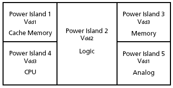
Although there are many advantages to higher levels of integration, SoC designers have traditionally sacrificed the ability to run different functions at different voltages and frequencies that they enjoyed at the PCB level. In response, the concept of power islands (also known as voltage islands) arose to allow areas of a single chip to operate at voltage levels and frequencies independent from one another. Figure 2 shows an example of power islands within an SoC design.

Figure 2: Example of Power Islands in an SoC
Power islands have been used in some high-volume commercial chips, including numerous cell phone ICs, the Intel processors with XScale technology and the Crusoe processor from Transmeta. For example, the Intel Pentium Processors with MMX Technology use two power islands, one (Vcc2) connected to the processor core and the other (Vcc3) connected to the I/O ring. However, such applications have required enormous amounts of internal development effort in libraries, tools and methodologies. Although many SoC design teams could benefit from the use of power islands, few companies can afford the resources to develop their own solutions.
Effective deployment of power islands within a synthesis-oriented design flow requires the development of custom EDA flows and many non-automated tasks. For example, voltage attributes may be specified in the RTL or in synthesis control files and used both to select the appropriate library cells and to pass information along with the post-synthesis netlist to the place and route process. Since not all voltages may be distributed to all areas of the chip, the use of power islands may have placement implications.
Although power islands were originally viewed as static, with the voltages decided at design time and fixed throughout chip operation, there is no fundamental reason why voltages cannot change over time. In fact, the many recent advances in power management have been addressing exactly this approach. Power supply ICs are now available with multiple voltage levels and tunable voltage levels. This is key enabling technology for the deployment of power islands. The PowerWise® technology from National Semiconductor has recently been standardized as the PowerWise Interface (PWI) to link power delivery, power distribution and power consumption together.
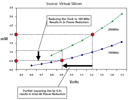
The goal of this work is to enable intelligent, adaptive power management, including the ability to make dynamic changes to the voltages and frequencies being applied to power islands. The idea is to supply each island with exactly the minimal amount of power and frequency to meet its performance and real-time response needs, which may change over time . As shown in Figure 3, the combination of varying voltage and operating frequency for a power island can have dramatic effects on power consumption.

Figure 3: Effects on Power of Varying Voltage and Frequency
For maximal results from this technology, decisions on performance needs must be made at a level with knowledge of the applications and their requirements, which means the computer operating system or device realtime operating system (RTOS). One example of effort in this direction is ARM’s Intelligent Energy Management (IEM) technology, which uses a combination of ARM’s processor cores (ARM9 and ARM11) and software to provide an integrated solution. The IEM software is actually adaptive, allowing the application software to “learn†how to lower the power at the correct times by scaling the voltage and frequency.
The Power Island Solution
Varying the voltages of individual functions within an SoC is clearly a significant advantage in power management. However, even greater flexibility is available if the clock frequencies of the individual functions can also be varied. Power islands provide this flexibility, isolating portions of a chip in terms of both voltage and frequency. With full control of voltage and clocks, each individual island can be managed for optimal power, performance and leakage current.
Given appropriate links to the operating system and its knowledge of application requirements, there are many scenarios in which power islands enable truly intelligent power management. For example, in a typical computer only a few applications require maximum performance. Many others, especially background tasks, have relaxed requirements. If a user running a high-end PC game steps away for a few minutes, it is likely that the system can scale down to a much lower power point until the game is resumed.
In addition, certain SoC functions may only be needed for specific applications. For example, many tasks may not perform any floating-point operations and so the floating-point unit within the processor could be run at a minimal voltage and frequency to conserve power. There are times when simply turning off the power to a unit is too drastic, since memory contents or other states information must be preserved. Power islands provide the flexibility to reduce the voltage and/or frequency to minimal levels.
The VIP™ PowerSaver™ standard cell products from Virtual Silicon are the first commercial semiconductor intellectual property (IP) offerings that enable mainstream design teams to take advantage of power islands. PowerSaver is an element of Virtual Silicon’s Mobilize Power Management IP offering. This makes the ideal solution for power management available to mainstream design teams, not just those very few large IDMs with the resources to develop custom libraries and IP.
The VIP PowerSaver library includes cells specifically optimized for high-performance, low-voltage operation as well as the level shifters and isolation gates that allow the designer to create electrically independent power islands capable of operating at different voltage levels and frequncies. The current library contains over 700 cells for the TSMC CL013G (130 nm) process, characterized for operation at 0.8, 1.0 and 1.2 volts. Libraries for additional processes will become available over time.
Summary
The demands for power management, especially in portable devices, have never been greater. Consumer and regulatory requirements are increasing more quickly than battery technology and traditional power management techniques can handle. As a result, a new approach is needed. Power islands, offering full control of voltage and frequency for individual functions within an SoC, are emerging as a solution of choice. The concept has been proven on large chips from a few vendors with extensive internal resources. With the introduction of Virtual Silicon’s Mobilize and VIP PowerSaver standard cell offerings, power islands are now available to every design team whose application requires the perfect balance between power and performance.
References
1. “A Combined Hardware-Software Approach for Low-Power SoCs: Applying Adaptive Voltage Scaling and Intelligent Energy Management Software†by Krisztian Flautner and David Flynn, DesignCon 2003 Proceedings, January 2003.
2. Powering Next-Generation Mobile Devices: A National Semiconductor White Paper, National Semiconductor, 2002.
3. Solving the Power Management Dilemma in System-On-Chip ASIC Design, IBM Technology Group, April 2002.
4. Voltage Guidelines for Pentium Processors with MMX Technology: Application Note AP-580, Intel, June 1997.
