by K. M. Sreekanth (India), Dahyot Lionel (France), Patnaik Rakesh (USA), Kumar Vinod (India)
Texas Instruments
Abstract :
Winning in the market place requires system development teams to put better product to the market ahead of competition. At the same time cost of the product needs to be reduced. Integration of more and more functionality into a single chip is becoming very important to achieve this objective. One of the key enablers in reducing time to market is to ensure that IPs used in the SOC are designed on-time and integration of these IPs into top level design is seamless. This paper discusses a comprehensive methodology developed and used for ensuring seamless IP integration with zero impact to the project schedules. The paper also discusses an innovative timing budget approach that helps concurrent development of top level design and modules/IPs used in the SOC.
I. INTRODUCTION
Intense competition to put new cellular phone products at lower cost into customer hands ahead of competitors is forcing system manufacturers to reduce cycle times. Complex System-On-Chip (SOC) designs are fast becoming a common place in today’s applications.
To reduce the time-to-market (TTM), IPs needed for the SOC must be developed in parallel to the top level design. This requires strong methodology and infrastructure which allows the SOC design team to define, communicate, and align on the requirements with IP teams. Methodology should also ensure that SOC design team gets the required data for the IPs that is needed to proceed with the current SOC design phase. Smooth integration of the IPs is also one of the key care-abouts in the SOC designs.
This paper discusses a comprehensive methodology developed and successfully implemented to enable parallel development of Hard IPs into SOC designs. This paper also discusses the quality checks and the release process introduced into the system to ensure smooth integration of IP into top level design.
II. SOC REQUIREMENTS & CHALLENGES
The main challenge of today’s SOC is to keep the cycle time as short as possible, while system complexities are increasing exponentially. They integrate several functionalities, partly new, with higher performance targets in same or reduced die sizes. Constant drive to reduce the costs of system is forcing to instantiate more and more analog and RF modules. A 10-15 million gates circuit unthinkable yesterday is real and common today. It is pushing the performance of EDA tools and computer platform to their limits; runtime often exceed the acceptable limits from project schedule perspective.
Furthermore, with the latest deep sub-micron technologies and in this specific market segment of cellular phone, the frequency increase is no longer the only parameter, designer needs to keep in mind. Power consumption, IR drops, electro-migration, cross-talk effects are very critical to ensure that system meets the performance targets. These deep sub micron effects need to be taken into account during the design. Design flows have been enhanced with new EDA tools to take care of them, but at the cost of increasing design cycle time and complexity.
Another trend that is becoming more common these days is distributed development model. Teams are formed based on domain of expertise. These teams may be spread across the world in different geographical locations to take advantage of non overlapping time zones, research and development costs. Use of contract houses is also becoming common. This poses serious challenges in managing the design. Issues that need to be addressed in this scenario ranges from ensuring proper communication across team members to mechanism of handing off data across the teams.
These factors drive to increase the complexity of IP development and integration. Systems, processes to address these issues are essential to ensure the success of the design. Scale of problem can be better appreciated from a recent SOC design, which integrated 23 IP blocks. These blocks were designed by nine teams in three continents. Approximately 10% of project time was lost because of IP integration issues.
III. SOLUTIONS
Methodology described below addresses this problem from two vectors - design and process techniques.
A. Design techniques
Design techniques are essentially based on hierarchical methodologies. This is used to split complexity and enable parallel development there by reducing the cycle time.
The technique commonly used is the partitioning. Process involves the division of full design into modules with respect to its nature (digital, mixed signal, RF), size, architecture, functionalities, power and frequencies domains, floor plan constraints and interconnects. This could be sometime also driven by tool runtime and capacity limitations.
Another technique consists of creation of abstract models (timing, physical, reliability etc) for the modules. This requires an initial partitioning definition. This method reduces the complexity of module visible at integration by providing abstracted views which represents the behaviors of the module. This results in cycle time reduction, simplification of data deliveries and easier integration and validation. This technique also helps to protect intellectual property. Drawback of this modeling technique is the lost of accuracy at analysis stage. Hence some margin should be kept to compensate it.
Reusability guidelines [1] are followed to isolate the IP model created from the integration context. This helps to reuse the IP core easily in other designs. This also contributes to reduce the effort required for timing closure.
The latest technique used is the budgeting. It applies on physical and timing models and is defined at specification level. It helps in providing early model, and early detection of potential design architecture or specification problems. Furthermore, if the budgets are kept till the end delivery, the subsequent margin between this reference and reality of the design could cover any late changes.
All of these techniques are key contributors in the realization of concurrent development model.
1) Scheme
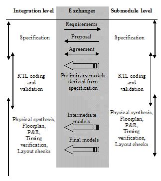
Fig.1.Concurrent development.
It defines succinctly the exchanges of a sub-module level with its integration level(s) with respect to their creation process phases.
2) Exchange process
Process is incremental in nature. Models are continuously refined in order to converge and achieve the design targets. But at this stage we should limit the number of delivery to avoid unnecessary exchanges of data, and limit the interdependencies between the integration and IP teams. Flow and process should provide flexibility and autonomy on both sides to drive their tasks.
That is why, for the exchange of IP model, three delivery stages are defined based on the need of chip design team to complete logical phases of the design.
A “preliminary†delivery stage, where models are derived from specification, and contain the budgeted values defined and agreed by both party. Using them, the integration team can get started with floor planning activity of the chip.
An “intermediate†delivery stage, where models can or not keep the budgeted values and/or be filled with extracted values from real design. The decision is made by the integration team based on the design constraints and the interface accuracy expectation. At that stage the models should have sufficient information for closing timing of design, get accurate power estimation, and pre-verify the layout effects to insure that we are converging to the final targets.
A “final†delivery stage – here the models are similar to the “intermediate†stage with signoff quality data for final tape out.
For each delivery stage, we define the expected minimum set of data by model type. Doing this helps in requesting and getting the appropriate data for the time they are needed, it also limits the risk to mix different model types at the assembly and insure to reach a targeted milestone.
Number of delivery stages could be changed based on the requirements of the project. This could be decided upfront during the start of the project.
3) IP creator responsibilities
One of the primary requirements for IP designer is to collect and merge the requests coming from multiple integration teams, align on the IP specification, the models request for delivery stages, the tool versions, and schedules.
IP and its models needs to be created, checked against requirements, then delivered to integration team. IP designer should also ensure that his module complies with re-usability requirements.
4) Integration team responsibilities
Integration team should define hierarchy of the design as soon as possible and fill its module needs and types (Soft macros, Hard Macros).
Then deliveries received from IP creator are checked to ensure on model quality and compliance with the particular requirements of its chip (PTV list, tool version …). QC log reports are also part of the delivery for better traceability on checks applied at creation stage.
B. Process techniques
Based on above design techniques, flows and process are put in place to guide, speed-up and check the design developments.
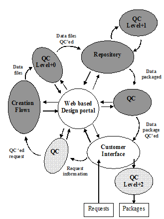
Fig.2. IP flow cycle.
It describes the overall IP development flow from request to package delivery. IP creator and IP user tasks are differentiated by different gray-scale.
The process starts with internal or external customers requests. They are handled and managed through a web interface, then verified and aligned. They are provided to the design teams at each stage of the data cycle with the main objective to ensure that request is compliant to the delivery stages.
All official versions of the data are stored in repositories managed by IP design teams. They are shared on request across the world for internal usage and packaged for external deliveries. In both cases, the web interface is updated with this new release information.
Between each main stage, quality checks are applied in order to detect as early as possible issues and reduce the iterative loops. QC reports are registered with the data and set as prerequisites for next stages. Asynchronous releases of different data types (simulation, physical, etc) from teams across the world for a given design are the common scenario. A consistency check is done between the new data and the data already present in the repository to ensure that only consistent data is added into repository. A compatibility table is created to reference the data coherent each others. The quality checks that are done in the process are described below
• Level+0 check
A check which can be performed on IP models without any information on the context in which the IP needs to be used is called as level0 check. In this bucket following checks are done
Checks which can be performed on IP models only when it is instantiated in the context of top level design is called as level1 check. The goal of this check is to simulate module integration. Basically this requires one or multiple IP to be instantiated in a dummy design and pushed through chip create flow. This identifies issues of models with respect to incompatibility of models with respect to tools used in the flow. Also this uncovers any unforeseen compatibility issue with chip create flow.
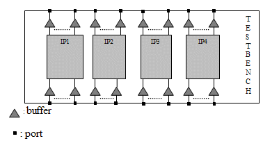
Fig.3. Level1 check
It shows the in-context QC applied on multiple IPs through a testbench.
• Level+2 check
This is design specific check. In this, checks on IP are done only with respect to top level design in which IP is getting used. These checkers help chip design team to perform quick check on the IP they received to ensure that they have all the information that is needed. As an example one of the checks which are very useful is to ensure that IP has Synopsys lib files for the corner in which top level design is being analyzed.
Another objective of the flow is to redirect any incident occurring or enhancement request as fast as possible, on data or tools directly to the right person. A corrective action is then elaborated and delivered through this interface.
All this process is based on EDA tools of the market selected for their capabilities and performances, and local scripts. In addition to active part of the code, monitoring features are also implemented to identify improvement areas and defined priorities of next flow releases.
IV. BENEFITS
System developed based on the framework described, is being used successfully within the organization. Key benefits seen so far :
V. CONCLUSION
This paper presents a comprehensive methodology to enable concurrent development and seamless integration of IPs resulting in SOC design cycle time reduction. Budget Timing approach is a key enabler for parallel development of IPs with SOC design. Automating the process which deals with IP model “request to development to QC to handoff†streamlines IP integration. This methodology has helped us to reduce significantly SOC design cycle time by providing formal framework, automation for the all the steps involved in development of IP blocks.
REFERENCES
[1] Michael Keating, Pierre Bricaud, “Reuse Methodology Manual For System-on-a-Chip Designs†, 2nd ed., Kluwer Academic Publishers (ISBN 0-7923-8558-6)
Texas Instruments
Abstract :
Winning in the market place requires system development teams to put better product to the market ahead of competition. At the same time cost of the product needs to be reduced. Integration of more and more functionality into a single chip is becoming very important to achieve this objective. One of the key enablers in reducing time to market is to ensure that IPs used in the SOC are designed on-time and integration of these IPs into top level design is seamless. This paper discusses a comprehensive methodology developed and used for ensuring seamless IP integration with zero impact to the project schedules. The paper also discusses an innovative timing budget approach that helps concurrent development of top level design and modules/IPs used in the SOC.
I. INTRODUCTION
Intense competition to put new cellular phone products at lower cost into customer hands ahead of competitors is forcing system manufacturers to reduce cycle times. Complex System-On-Chip (SOC) designs are fast becoming a common place in today’s applications.
To reduce the time-to-market (TTM), IPs needed for the SOC must be developed in parallel to the top level design. This requires strong methodology and infrastructure which allows the SOC design team to define, communicate, and align on the requirements with IP teams. Methodology should also ensure that SOC design team gets the required data for the IPs that is needed to proceed with the current SOC design phase. Smooth integration of the IPs is also one of the key care-abouts in the SOC designs.
This paper discusses a comprehensive methodology developed and successfully implemented to enable parallel development of Hard IPs into SOC designs. This paper also discusses the quality checks and the release process introduced into the system to ensure smooth integration of IP into top level design.
II. SOC REQUIREMENTS & CHALLENGES
The main challenge of today’s SOC is to keep the cycle time as short as possible, while system complexities are increasing exponentially. They integrate several functionalities, partly new, with higher performance targets in same or reduced die sizes. Constant drive to reduce the costs of system is forcing to instantiate more and more analog and RF modules. A 10-15 million gates circuit unthinkable yesterday is real and common today. It is pushing the performance of EDA tools and computer platform to their limits; runtime often exceed the acceptable limits from project schedule perspective.
Furthermore, with the latest deep sub-micron technologies and in this specific market segment of cellular phone, the frequency increase is no longer the only parameter, designer needs to keep in mind. Power consumption, IR drops, electro-migration, cross-talk effects are very critical to ensure that system meets the performance targets. These deep sub micron effects need to be taken into account during the design. Design flows have been enhanced with new EDA tools to take care of them, but at the cost of increasing design cycle time and complexity.
Another trend that is becoming more common these days is distributed development model. Teams are formed based on domain of expertise. These teams may be spread across the world in different geographical locations to take advantage of non overlapping time zones, research and development costs. Use of contract houses is also becoming common. This poses serious challenges in managing the design. Issues that need to be addressed in this scenario ranges from ensuring proper communication across team members to mechanism of handing off data across the teams.
These factors drive to increase the complexity of IP development and integration. Systems, processes to address these issues are essential to ensure the success of the design. Scale of problem can be better appreciated from a recent SOC design, which integrated 23 IP blocks. These blocks were designed by nine teams in three continents. Approximately 10% of project time was lost because of IP integration issues.
III. SOLUTIONS
Methodology described below addresses this problem from two vectors - design and process techniques.
A. Design techniques
Design techniques are essentially based on hierarchical methodologies. This is used to split complexity and enable parallel development there by reducing the cycle time.
The technique commonly used is the partitioning. Process involves the division of full design into modules with respect to its nature (digital, mixed signal, RF), size, architecture, functionalities, power and frequencies domains, floor plan constraints and interconnects. This could be sometime also driven by tool runtime and capacity limitations.
Another technique consists of creation of abstract models (timing, physical, reliability etc) for the modules. This requires an initial partitioning definition. This method reduces the complexity of module visible at integration by providing abstracted views which represents the behaviors of the module. This results in cycle time reduction, simplification of data deliveries and easier integration and validation. This technique also helps to protect intellectual property. Drawback of this modeling technique is the lost of accuracy at analysis stage. Hence some margin should be kept to compensate it.
Reusability guidelines [1] are followed to isolate the IP model created from the integration context. This helps to reuse the IP core easily in other designs. This also contributes to reduce the effort required for timing closure.
The latest technique used is the budgeting. It applies on physical and timing models and is defined at specification level. It helps in providing early model, and early detection of potential design architecture or specification problems. Furthermore, if the budgets are kept till the end delivery, the subsequent margin between this reference and reality of the design could cover any late changes.
All of these techniques are key contributors in the realization of concurrent development model.
1) Scheme

Fig.1.Concurrent development.
It defines succinctly the exchanges of a sub-module level with its integration level(s) with respect to their creation process phases.
2) Exchange process
Process is incremental in nature. Models are continuously refined in order to converge and achieve the design targets. But at this stage we should limit the number of delivery to avoid unnecessary exchanges of data, and limit the interdependencies between the integration and IP teams. Flow and process should provide flexibility and autonomy on both sides to drive their tasks.
That is why, for the exchange of IP model, three delivery stages are defined based on the need of chip design team to complete logical phases of the design.
A “preliminary†delivery stage, where models are derived from specification, and contain the budgeted values defined and agreed by both party. Using them, the integration team can get started with floor planning activity of the chip.
An “intermediate†delivery stage, where models can or not keep the budgeted values and/or be filled with extracted values from real design. The decision is made by the integration team based on the design constraints and the interface accuracy expectation. At that stage the models should have sufficient information for closing timing of design, get accurate power estimation, and pre-verify the layout effects to insure that we are converging to the final targets.
A “final†delivery stage – here the models are similar to the “intermediate†stage with signoff quality data for final tape out.
For each delivery stage, we define the expected minimum set of data by model type. Doing this helps in requesting and getting the appropriate data for the time they are needed, it also limits the risk to mix different model types at the assembly and insure to reach a targeted milestone.
Number of delivery stages could be changed based on the requirements of the project. This could be decided upfront during the start of the project.
3) IP creator responsibilities
One of the primary requirements for IP designer is to collect and merge the requests coming from multiple integration teams, align on the IP specification, the models request for delivery stages, the tool versions, and schedules.
IP and its models needs to be created, checked against requirements, then delivered to integration team. IP designer should also ensure that his module complies with re-usability requirements.
4) Integration team responsibilities
Integration team should define hierarchy of the design as soon as possible and fill its module needs and types (Soft macros, Hard Macros).
Then deliveries received from IP creator are checked to ensure on model quality and compliance with the particular requirements of its chip (PTV list, tool version …). QC log reports are also part of the delivery for better traceability on checks applied at creation stage.
B. Process techniques
Based on above design techniques, flows and process are put in place to guide, speed-up and check the design developments.

Fig.2. IP flow cycle.
It describes the overall IP development flow from request to package delivery. IP creator and IP user tasks are differentiated by different gray-scale.
The process starts with internal or external customers requests. They are handled and managed through a web interface, then verified and aligned. They are provided to the design teams at each stage of the data cycle with the main objective to ensure that request is compliant to the delivery stages.
All official versions of the data are stored in repositories managed by IP design teams. They are shared on request across the world for internal usage and packaged for external deliveries. In both cases, the web interface is updated with this new release information.
Between each main stage, quality checks are applied in order to detect as early as possible issues and reduce the iterative loops. QC reports are registered with the data and set as prerequisites for next stages. Asynchronous releases of different data types (simulation, physical, etc) from teams across the world for a given design are the common scenario. A consistency check is done between the new data and the data already present in the repository to ensure that only consistent data is added into repository. A compatibility table is created to reference the data coherent each others. The quality checks that are done in the process are described below
• Level+0 check
A check which can be performed on IP models without any information on the context in which the IP needs to be used is called as level0 check. In this bucket following checks are done
- Presence of required IP models
- Syntax check on files, models of IP to be delivered to chip create flow
- Check for correctness of models with respect to chip create flow requirements
- Consistency of information across different models. Ex. Port names
Checks which can be performed on IP models only when it is instantiated in the context of top level design is called as level1 check. The goal of this check is to simulate module integration. Basically this requires one or multiple IP to be instantiated in a dummy design and pushed through chip create flow. This identifies issues of models with respect to incompatibility of models with respect to tools used in the flow. Also this uncovers any unforeseen compatibility issue with chip create flow.

Fig.3. Level1 check
It shows the in-context QC applied on multiple IPs through a testbench.
• Level+2 check
This is design specific check. In this, checks on IP are done only with respect to top level design in which IP is getting used. These checkers help chip design team to perform quick check on the IP they received to ensure that they have all the information that is needed. As an example one of the checks which are very useful is to ensure that IP has Synopsys lib files for the corner in which top level design is being analyzed.
Another objective of the flow is to redirect any incident occurring or enhancement request as fast as possible, on data or tools directly to the right person. A corrective action is then elaborated and delivered through this interface.
All this process is based on EDA tools of the market selected for their capabilities and performances, and local scripts. In addition to active part of the code, monitoring features are also implemented to identify improvement areas and defined priorities of next flow releases.
IV. BENEFITS
System developed based on the framework described, is being used successfully within the organization. Key benefits seen so far :
- SOC Program Management can keep tab on the progress of IP development across different teams. Corrective actions can be initiated at the earliest
- SOC designers can communicate requirements; receive the deliverables from IP designers through formal mechanism.
- Specification of timing budgets helps the IP development team to start early and integration of the block to the top level will be smooth.
- IP designers can use integration flow to ensure that they adhere to all the flow requirements before they release the IP to top level design team
- All stakeholders are well aware of the progress and issues if any
V. CONCLUSION
This paper presents a comprehensive methodology to enable concurrent development and seamless integration of IPs resulting in SOC design cycle time reduction. Budget Timing approach is a key enabler for parallel development of IPs with SOC design. Automating the process which deals with IP model “request to development to QC to handoff†streamlines IP integration. This methodology has helped us to reduce significantly SOC design cycle time by providing formal framework, automation for the all the steps involved in development of IP blocks.
REFERENCES
[1] Michael Keating, Pierre Bricaud, “Reuse Methodology Manual For System-on-a-Chip Designs†, 2nd ed., Kluwer Academic Publishers (ISBN 0-7923-8558-6)
