Tokyo, March 8, 2017 - NEC Corporation (NEC) and the National Institute of Advanced Industrial Science and Technology (AIST) today announced the development of an NB-FPGA (Note 1) that incorporates NanoBridge metal atom migration-type switch technology utilizing TIA (Note 2), an open innovation hub operated by five institutes in Tsukuba and Tokyo. This original NEC product featuring high radiation tolerance is expected to contribute to the use of LSIs in space.
Current FPGAs (SRAM-type FPGAs, Note 3), when used in space, pose the problem of changes occurring to the information written in the SRAM and malfunctions being caused due to the effects of radiation. However, this NanoBridge technology enables a tenfold improvement over the power efficiency of conventional FPGAs as well as providing them with high radiation tolerance.
NEC has conducted an operation demonstration jointly with the Japan Aerospace Exploration Agency (JAXA), using the newly developed NB-FPGA in a tough radioactive terrestrial environment. As a result, it has confirmed that the ON and OFF states of the NanoBridge remain unchanged, whether radiation is delivered or not. "Based on the result, NEC expects that the NanoBridge will be able to reduce the frequency of errors caused by radiation to one percent or less and contribute to the creation of an LSI that offers high radiation tolerance and ultra-low power consumption simultaneously," said Yuichi Nakamura, General Manager, System Platform Research Laboratories, NEC Corporation.
This NB-FPGA was developed jointly by NEC and AIST, building on the success of NEDO's "Low-power Electronics Association & Project (LEAP)," and is one of the TIA's open innovation achievements.
Going forward, NEC and JAXA will validate the usability and reliability of the NB-FPGA by incorporating it in the Innovative Satellite Technology Demonstration 1, which will be launched in FY2018.
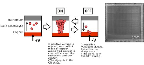
 Fig. 1: Operation mechanism of NanoBridge (left), NB-FPGA chip (right)
NanoBridge Radiation Resistance
Devices used in satellites are required to be extremely reliable. Even so, they are susceptible to circuitry failures called single event phenomena due to the effects of strong radiation in space. The occurrence of failures due to radiation poses a similar challenge in terrestrial communication devices as well. For example, if radiation is delivered to an LSI, an electrical charge occurs in the semiconductor substrate. As a result, a failure occurs to the SRAMs in FPGAs that record information based on the amount of charge, causing a change in the circuit configuration.
The NanoBridge uses the cross-link of metal atoms in a solid electrolyte to place the signals into the ON or OFF state (Fig.1). The ON or OFF state is maintained even after voltage is released. The cross-link created by metal atoms in the NanoBridge is free from the impact of electrical charges generated by the delivery of radiation. Accordingly, the possibility of rewriting is extremely remote in the circuit of NB-FPGA, even in a space environment that is exposed to a large amount of radiation, thereby making the product extremely reliable.
Demonstration Experiment in Space
The NB-FPGA will be incorporated in the Innovative Satellite Technology Demonstration 1, which will be launched in FY2018, and a demonstration experiment of compressing and transmitting camera-captured images through the NB-FPGA will be carried out in a harsh environment.
NB-FPGA for which the evaluation was performed
Going forward, NEC will develop NB-FPGA for application with satellite systems by utilizing the evaluation results in the Innovative Satellite Technology Demonstration program conducted by JAXA. NEC applies NB-FPGA to highly-reliable apparatus in harsh environments on the ground, i.e., robots, automobiles and commutations equipment (Note 6).
***
About NEC Corporation
NEC Corporation is a leader in the integration of IT and network technologies that benefit businesses and people around the world. By providing a combination of products and solutions that cross utilize the company's experience and global resources, NEC's advanced technologies meet the complex and ever-changing needs of its customers. NEC brings more than 100 years of expertise in technological innovation to empower people, businesses and society. For more information, visit NEC at http://www.nec.com.
The NEC Group globally provides "Solutions for Society" that promote the safety, security, efficiency and equality of society. Under the company's corporate message of "Orchestrating a brighter world," NEC aims to help solve a wide range of challenging issues and to create new social value for the changing world of tomorrow. For more information, please visit